



eGaN FET for Lidar - Maximizing Laser Driver Performance Part 1
 Published2019.09.25 09:51
Over the past several years, Time-of-Flight (ToF) distance measurement, a specific type of lidar, has been widely adopted. When a laser is used as the optical source, it enables distance measurement even to small sections at far distances. When used with adjustable optics, it can measure the distance to a specific point and implement a three-dimensional map of the object.
EPC has developed the EPC9126 and EPC9126HC laser drivers to provide the performance benefits of eGaN FETs to lidar systems and enhance the technology level of lidar. Although the basic principle of this laser driver appears simple, parasitic components that many engineers overlook in design give it high-speed, high-voltage, and high-current characteristics.
This technical article was written to provide in-depth information on laser driver design so that users can maximize the benefits of the driver and to answer commonly raised questions.
Basic Design Process
We can now utilize the information covered in the previous article to perform a resonant lidar driver design. Let us start with some laser pulse specifications typically required in system design.
The requirements are as follows:
▲Pulse peak amplitude IDLpk
▲FWHM (Full Width Half Maximum) pulse width tw
▲Pulse repetition frequency PRF
▲Laser diode forward voltage drop VDLF
Once the basic pulse requirements are selected, the next element needed to complete the design is the power loop inductance L1. The determination of L1 was discussed in the previous article, but for now let us assume we have a good estimate value.
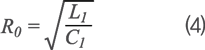

Using equations (4) and (6) to determine the value of the resonant capacitor C1, we obtain the following:

The value of the recharge resistor R1 is determined from equation (2), as follows:


Since τchrg≫tres, we only need to select a sufficient value for τchrg. Generally, the R1 value does not require precise determination because thermal limiting must be applied such that the pulse duty cycle is less than 1%.

Finally, the required bus voltage VIN is determined through equation (7), and IDLpk is also used together in selecting an appropriate part number for FET Q1. Through equations (7), (8), and (9), the remaining values needed to complete the design are determined.
Determining Power Loop Inductance
We have already seen that the required input voltage increases nearly linearly with respect to the laser inductance, and the input voltage determines the ratings of the FET and capacitor.
The laser driver bus voltage also comes from elsewhere, most likely from another boost converter in the circuit. The lower L1 is, the simpler and more cost-effective the remaining design becomes.
The key principles for minimizing PCB inductance are detailed in reference1), which introduces several useful techniques for reducing layout inductance.
This material shows that with chip-scale packages of eGaN FETs, the contribution to the power loop inductance of the FET, PCB, bus capacitance, and current sense shunt (if needed) can be maintained below 1nH, and values approaching less than 500pH are achievable.
The parasitic inductance of the EPC9126xx is approximately 1nH depending on the FET and load mounting location. This value is higher than the best achievable value, particularly because it is a compromise to increase design flexibility to accommodate different laser packages.
Let us now examine other inductance sources.
One of the major sources is the laser itself. As noted earlier, through-hole lasers are expected to contribute approximately 5nH in the best case, but often much higher. Surface-mount lasers contribute approximately 1-3nH, meaning the laser becomes the dominant inductance source.
Most of the laser inductance originates from the laser package, including wire bonding. Laser manufacturers are well aware that laser package inductance can overwhelm performance, so advancements in this area are expected in the near future.
Unfortunately, the value of L1 is difficult to know precisely early in the design phase. Therefore, some iterative work may be necessary. By considering additional voltage margin for the FET in the initial design, some of the unanticipated inductance can be overcome.
EPC9126xx Hardware Driver Design
A typical connection diagram for the EPC9126xx laser driver is shown in [Figure 8].
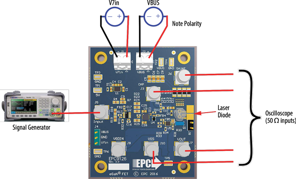
A complete description of the connections and operation can be found in the Quick Start Guide2)3), and here we will briefly review this diagram.
All signal I/O use SMA connectors. This design includes voltage test points obtained from J3, J7, J9, J10 with embedded transmission line probes. The output of the current measurement shunt can be accessed via J6.
Design details, including Gerber layout files and complete schematics, can be found in references4)5). The layout was designed to minimize total inductance according to the principles described in reference1).
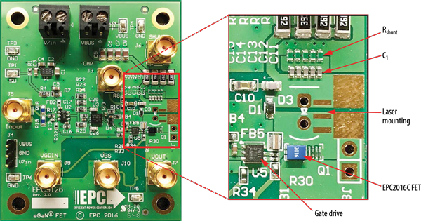
EPC9126 Laser Driver for Experimental Verification
A photograph of the driver and enlarged views of key portions of the design are shown in [Figure 9].
To minimize inductance L1, the energy storage capacitor C1 (C11, C12, C13, C14, C15 on the PCB) and current measurement shunt (R12, R13, R14, R15, R16) are composed of five 0402-size surface-mount packages connected in parallel.
The spacing between the top plane and ground plane is 250μm (10mil) to minimize inductance. Blind and buried vias and microvias were not used to minimize cost.
To achieve excellent shunt performance for current measurement, the shunt resistor had to be mounted upside down, reducing the shunt equivalent series inductance from 200pH to 40pH, resulting in a four-fold increase in shunt bandwidth.6) Additional discussion on this will be detailed in the current sensing section.
Experimental Results
Both the EPC9126 and EPC9126HC were tested using the Excelitas TPGAD1S09H surface-mount laser, currently the lowest inductance surface-mount high-output pulse laser readily available at the time of writing this article. In each case, circuit testing yielded an input voltage of 75V.
EPC9126
The power loop inductance L1 was estimated at 2.3nH. With a design of IDLpk=35A and 3.5ns pulse width, C1=1.2nF and VIN=60V. The capacitor value used was C1=1.1nF, the closest standard part value available. NP0/C0G ceramic capacitors were used due to stable capacitance and low losses.
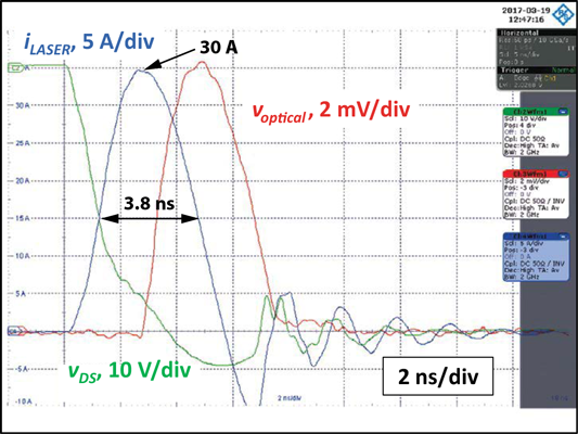
Test results for VIN=75V are shown in [Figure 10]. Peak current, IDLpk=35A, is reached at tw=3.4ns. This corresponds to the maximum power input for the laser PDLpk>300W. The discrepancy between results and calculations occurs because of different capacitance values and inductance estimation errors, additional voltage drops across the shunt, and the fact that the laser diode forward voltage drop is not actually a fixed value.
EPC9126HC
The power loop inductance L1 was estimated at 2.0nH, reduced due to the larger footprint of the EPC2001C compared to the EPC2016C. With a design of IDLpk=70A and 5ns pulse width, C1=2.85nF and VIN=78V. The capacitor value used was C1=2.8nF, the closest standard part value available. NP0/C0G ceramic capacitors were used due to stable capacitance and low losses.
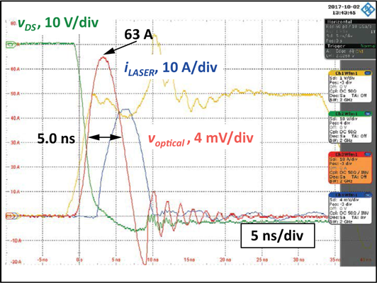
Test results for VIN=75V are shown in [Figure 11]. Peak current, IDLpk=63A, is reached at tw=5.0ns. This corresponds to the maximum power input for the laser PDLpk>1300W. The discrepancy between results and calculations occurs because of slightly different capacitance values and inductance estimation errors, additional voltage drops across the shunt, and the fact that the laser diode forward voltage drop is not actually a fixed value.
Tips and Useful Information for the 9126
The EPC9126xx is highly flexible and can be used to try new ideas or gain detailed insight into the actual behavior of components for fast, high-current pulses. In this section, we will discuss design details and provide additional recommendations for different directions.
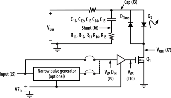
[Figure 12] is the block diagram of the EPC9126xx and provides a useful reference for this section.
In the final installment that follows, we will explore RF techniques for the high-speed performance of laser pulse drivers, specifically the use of controlled impedance and the standard 50Ω impedance for cables and measurements.
References
1) D. Reusch and J. Strydom, "Understanding the effect of PCB layout on circuit performance in a high frequency gallium nitride based point of load converter," 2013 Twenty-Eighth Annual IEEE Applied Power Electronics Conference and Exposition (APEC), 2013, pp. 649–655.
2) Efficient Power Conversion Corp., "EPC9126 Lidar Development Board Quick Start Guide, Rev. 2.5," 2016.
3) Efficient Power Conversion Corp., "EPC9126HC Lidar Development Board Quick Start Guide, Rev. 1.0," 2017.
4) EPC9126 Lidar Demo Board (https://epc-co.com/epc/Products/DemoBoards/EPC9126.aspx)
5) EPC9126HC Lidar Demo Board (https://epc-co.com/epc/Products/DemoBoards/EPC9126.aspx)
6) J. Glaser, " High Power Nanosecond Pulse Laser Driver using a GaN FET", PCIM Europe 2018 Proceedings, 2018.
#Regarding this article, e4ds.com is conducting experimental discussions on GaN technology for lidar. If you have questions about this technology or wish to submit additional contributions, please leave a comment below.
관련뉴스
Velodyne Lidar Provides Lidar Technology for Karta's Stencil 2-32 Mobile Mapping System
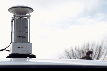
Velodyne's lidar technology is embedded in Kaarta's Stencil 2-32 ground surface mapping solution. The Stencil 2-32 accurately surveys ground surface at a lower cost than existing mobile mapping systems, mapping curbs, manholes, signage, poles, and other features. The Stencil platform can assist not only urban planning for infrastructure improvement but also parking and traffic management. AllVision in the United States was able to analyze curb occupancy within Pittsburgh's Strip District, known for high on-street parking demand, using data from autonomous vehicle developers together with the Stencil 2-32.
2019.07.18by 이수민 기자
.png)
KETI Localizes Autonomous Driving LiDAR Sensors for Unmanned Transport Robots
KETI has succeeded in localizing a scanning lidar sensor for SLAM used in autonomous navigation of smart factory autonomous mobile robots. In the past, AGVs operated using a traditional SLAM method that recognized artificial markings such as optical recognition metal wires or magnetic lines attached to the floor and traveled along predetermined paths. Recently, AGVs using autonomous navigation methods that recognize position using lidar without separate markings and further create and utilize surrounding maps have become commonplace. Until now, scanning lidar sensors for SLAM had to rely on Japanese and German products priced around 2 to 3 million won. The scanning lidar sensor for autonomous navigation of unmanned mobile robots developed by KETI this time is capable of 180° detection and can detect objects as small as 10cm at a maximum distance of 30m.
2019.08.26by 최인영 기자
eGaN FETs for LiDAR - Getting the Most Out of Laser Drivers Theory
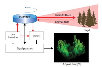
Lidar is a form of radar that generates electromagnetic waves in a broad spectrum. Over the past several years, Time-of-Flight (TOF) distance measurement, one specific form of lidar, has been widely adopted. When a laser is used as the optical source, distance measurements can be taken even to small areas at far distances, and when used with adjustable optical devices, the distance to that point can be measured and a three-dimensional map of the object can be implemented.
2019.09.09by 명세환 기자

Intel Unveils Next-Generation 'Core Ultra Series 3' and vPro Platform for Enterprise PCs
Intel has officially unveiled the "Intel Core Ultra Series 3" for next-generation enterprise PCs and the latest vPro platform, addressing a wide range of demands from enterprise notebooks to high-performance workstations.
2026.03.26by 배종인 기자

ROHM Launches ESD Protection Diode Compatible with High-Speed Interfaces of 10Gbps or Higher
Semiconductor specialist ROHM has developed the 'RESDxVx series' of ESD (electrostatic discharge) protection diodes capable of responding to next-generation high-speed data communication environments exceeding 10Gbps, simultaneously enhancing both signal quality maintenance required in high-speed interfaces and IC protection performance.
2026.03.26by 배종인 기자











