



ST Launches Ultra-Compact, High-Performance Global Shutter Image Sensor
 Published2020.03.30 11:35
Implementing unrivaled BSI global shutter pixels with die stacking technology
STMicroelectronics has launched a new high-speed image sensor to support next-generation smart computer vision applications.
Use Global Shutter mode, which is primarily used for distortion-free image capture when moving scenes or near-infrared lighting are required.
Rolling shutters, which capture pixel data one line at a time, often result in distorted moving images or require additional correction work, whereas global shutter sensors can store all pixel data of each frame simultaneously.
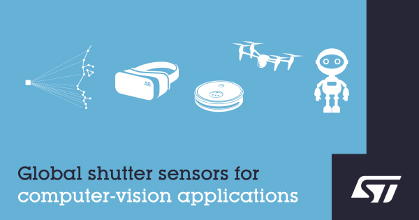
▲ Global-shutter machine-vision sensors <Image=ST>
The sensors introduced this time are the VD55G0 with 640 x 640 pixels and the VD56G3 with 1.5M pixels (1124 x 1364), achieving the smallest resolutions on the market at 2.6mm x 2.5mm and 3.6mm x 4.3mm.
Low inter-pixel crosstalk is possible across all wavelengths, including near-infrared, ensuring clear images with high contrast. The optical flow processing function built into the VD56G3 can calculate motion vectors without processing on a host computer, making it suitable for various applications such as augmented and virtual reality (AR/VR), SLAM (Simultaneous Localization and Mapping), and 3D scanning.
ST's advanced pixel technologies, including full Deep Trench Isolation (DTI), enable ultra-small 2.61㎛ x 2.61㎛ pixels on a single wafer layer, combining low Parasitic Light Sensitivity (PLS), excellent Quantum Efficiency (QE), and low crosstalk.
In addition, by implementing small pixels on a back-illuminated (BSI) wafer and vertically stacking optical sensors and related signal processing circuits at the bottom of the die, space can be reduced while minimizing sensor size and embedding key functions such as a fully autonomous optical flow block.
The bottom die is manufactured using ST's 400nm technology and integrates digital and analog circuits. The high-density, low-power digital circuits are equipped with all hardware features, including an exposure algorithm for statistics collected from up to 336 regions, as well as automatic defect correction and automatic dark correction.
The fully autonomous low-power optical flow block can calculate 2,000 motion vectors at a speed of 60fps. The built-in vector generation function is very useful for augmented and virtual reality or robotics, and supports SLAM or 6DoF (Six Degrees of Freedom) applications, especially on host systems with limited processing power.
This sensor supports multi-frame context through sequencing programming functions as well as full lighting control, and is equipped with an integrated temperature sensor, I2C high-speed mode+ control, fault correction, windowing, binning, and MIPI CSI-2 data interface.
Comments
Related news

Infineon and Qualcomm Provide High-Quality Standard Solutions for 3D Authentication
Infineon has collaborated with Qualcomm to develop a reference design for 3D authentication based on the Qualcomm Snapdragon 865 mobile platform. This reference design, which incorporates Infineon's REAL 3D RoF sensor, supports standardized and seamless design integration for smartphone manufacturers.
2020.03.11by 최인영 기자
Launch of two frame grabbers for MIPI CSI-2 image sensors
Introspect has launched two framegrabber solutions for verification and optimization of image sensors that comply with the MIPI Alliance CSI-2 SM standard and are based on the MIPI Alliance C-PHY SM and D-PHY SM physical layers. The two new solutions enable fast frame capture and image processing across all host computer platforms and support the latest MIPI Alliance specifications.
2020.03.23by 이수민 기자

Markbase Time Series DBMS v6.0 Announced, Targeting 100 Million IIoT Sensor Data Transactions Per Second
A time series DBMS is a specialized-purpose DBMS designed for processing time series data generated at regular time intervals. Mackebase announced Mackebase v6.0, a time series DBMS that supports real-time processing of ultra-high-capacity sensor data generated from IIoT devices. To enable real-time input and query of large-capacity data reaching millions of records per second, it employs tag and time-based index configuration and high-efficiency compression technology.
2020.03.24by 이수민 기자

Intel Unveils Next-Generation 'Core Ultra Series 3' and vPro Platform for Enterprise PCs
Intel has officially unveiled the "Intel Core Ultra Series 3" for next-generation enterprise PCs and the latest vPro platform, addressing a wide range of demands from enterprise notebooks to high-performance workstations.
2026.03.26by 배종인 기자

ROHM Launches ESD Protection Diode Compatible with High-Speed Interfaces of 10Gbps or Higher
Semiconductor specialist ROHM has developed the 'RESDxVx series' of ESD (electrostatic discharge) protection diodes capable of responding to next-generation high-speed data communication environments exceeding 10Gbps, simultaneously enhancing both signal quality maintenance required in high-speed interfaces and IC protection performance.
2026.03.26by 배종인 기자











