


KLA Announces eSL10 Electron-Beam Patterned Wafer Defect Inspection System
 Published2020.07.22 10:38
Bringing forward the launch of high-performance logic and memory semiconductor chips
KLA announced on the 21st its newly developed e-beam patterned-wafer defect inspection system, eSL10™.
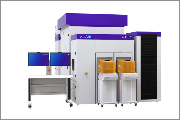
The eSL10 is designed to accelerate time-to-market for high-performance logic and memory semiconductor chips, including those manufactured using extreme ultraviolet (EUV) lithography, by detecting and reporting defects that cannot be detected by conventional optical equipment or other electron-beam defect inspection platforms.
Yellowstone™ scanning mode can acquire 10 billion pixels of data per scan, allowing high-speed operation while maintaining high resolution. Therefore, efficient inspection of suspected hot spots or detection of defects in a wide area is possible.
Simul-6™ sensor technology collects surface, topography, material contrast, and deep trench information in a single scan, reducing the time required to identify different defect types in challenging device structures and materials.
Customers can build powerful defect detection and monitoring solutions by combining the eSL10 system, which uses deep learning algorithms, with KLA’s 39xx (5th generation) and 29xx (4th generation) wideband optical wafer defect inspection systems.
“Previous e-beam inspection systems have limited their potential for practical applications by offering either high sensitivity or ultra-high speed,” said Amir Azordegan, general manager of KLA’s e-beam division. “The eSL10 system dramatically increases e-beam inspection capability by utilizing a single, high-current-density electron beam.”
Meanwhile, customers of the eSL10 system can benefit from KLA’s global comprehensive service network.
Comments
Related news
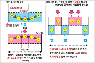
Memory semiconductor integration will increase 1,000 times compared to now
Professor Lee Jun-hee's research team at UNIST has presented a principle that can increase the integration density of memory semiconductors by more than 1,000 times. Conventional memory uses domains of tens of nanometers in size to store 1 bit through inter-atomic elastic interactions, but by utilizing the phenomenon presented by the research team, inter-atomic elastic interactions disappear when voltage is applied, making it possible to store data in individual atoms.
2020.07.03by 이수민 기자
"Automotive power design starts with understanding MOSFETs"
Vehicle electrification is not occurring only in the powertrain. With advances in autonomous driving, infotainment, and other technologies, the ratio of power semiconductor integration in vehicles is steadily increasing. Developers must now develop the ability to understand AEC-Q101 and read power component datasheets in order to avoid performance degradation, cost increases, and design errors in automobiles and automotive electrical components.
2020.07.13by 이수민 기자

Analog semiconductor industry's 2nd-ranked ADI acquires 7th-ranked Maxim
ADI is acquiring Maxim Integrated. The combined company is valued at approximately $68 billion, including debt. ADI's current market capitalization is approximately $48 billion, and Maxim's is approximately $17 billion. ADI previously acquired Linear Technology in 2016.
2020.07.14by 이수민 기자
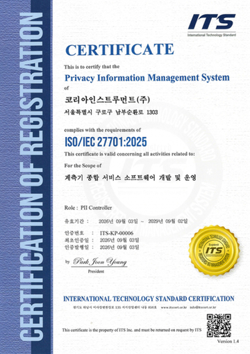
Korea Instrument, KOLAS Accredited Calibration Agency First to Simultaneously Acquire ISO/IEC 27,001·27,701
Korea Instrument has become the first among KOLAS accredited calibration agencies to simultaneously acquire ISO/IEC 27,001 and ISO/IEC 27,701 certifications. Through its proprietary platforms CWIZ Enterprise and CWIZ Partners, the company has embedded information security and personal data protection requirements across all business processes including customer information, equipment data, and calibration reports, with plans to continuously advance its management system through regular audits and security inspections.
2026.10.12by 배종인 기자

TeamViewer One, IT Incident Automation Workflow and Resolution Center Enhanced
TeamViewer has added IT incident automation capabilities and an advanced Resolution Center to its integrated digital workplace management platform 'TeamViewer ONE'. Recurrent service disruptions, configuration errors, and capacity shortages are automatically handled according to preset policies, and device status verification through script deployment can be managed in a unified interface, significantly reducing repetitive tasks for IT teams.
2026.10.12by 배종인 기자











