



Semiconductor packaging materials market projected to grow at an average annual rate of 3.4%.
 Published2020.07.29 10:22
Projected to reach $20.8 billion in 2024
The semiconductor industry is expected to continue growing, driven by big data, high-performance computing, AI, edge computing, advanced memory, 5G, and automotive semiconductors. Packaging materials are a key component directly linked to the performance and reliability of next-generation semiconductors.

The Semiconductor Equipment and Materials International (SEMI) announced on the 29th that the semiconductor packaging materials market size is expected to grow from $17.6 billion in 2019 to $20.8 billion in 2024, recording an average annual growth rate of 3.4%, citing the latest 'Global Semiconductor Packaging Materials Outlook' report from electronics industry research firm TechSearch.
Laminate substrates, the largest segment in the packaging materials sector, are expected to grow at a compound annual growth rate of more than 5% from 2019 to 2024, driven by increasing demand for system-in-package (SIP) and high-performance semiconductors. Dielectric materials used in wafer-level packaging are expected to grow at an average annual rate of 9%.
Meanwhile, the packaging trend toward smaller and thinner packaging to improve semiconductor performance is expected to slow the growth of leadframe, die attach, and encapsulant materials.
As semiconductor packaging technology continues to evolve, opportunities are expected to emerge in the materials market in the following areas over the next few years.
▲New substrates supporting high-density, miniaturized bumps ▲Low-k laminate materials (low Dk) and low-dielectric factor (low Df) laminate materials for 5G mmWave ▲Coreless based on MIS (Molded Interconnect Solution/System) leadframe technology ▲Mold compound providing underfill for copper pillar flip chips ▲Miniaturization of resin material particles to solve miniaturization problems ▲Die attach materials below 5µm with no-to-low resin bleed and no-to-low outgassing ▲Low-k materials required for high-frequency applications ▲Void-free deposition and low-overburden deposition required for Through-Silicon Via (TSV)
According to the report, the semiconductor materials market is expected to see the following growth prospects from 2019 to 2024:
△The global semiconductor packaging laminate substrate market will record a compound annual growth rate of 5% on a square meter basis △The average annual growth rate of total lead frame shipments will be slightly over 3% △The average annual growth rate of LFCSP (QFN type) will reach approximately 7% △The average annual growth rate of encapsulation material revenue will be approximately 3% due to the increasing demand for small and thin form factors △Die attach material revenue is expected to grow at a CAGR of approximately 4% △Solder ball revenue is expected to grow at a CAGR of 3% △The wafer-level packaging dielectric materials market is expected to grow at a CAGR of 9% △The wafer-level plating chemical market is expected to grow at a CAGR of 7%
Comments
Related news

The semiconductor materials market size decreased by 1.1% last year compared to the year before.
In 2019, the global semiconductor materials market size recorded $52.1 billion, down 1.1% compared to 2018. According to SEMI, the materials used in the front-end in 2019 decreased from $33.0 billion in 2018 to approximately $32.8 billion, while packaging materials declined 2.3% from $19.7 billion in 2018 to approximately $19.2 billion in 2019. Materials that increased in 2019 were found to be only substrates and other packaging materials.
2020.04.01by 이수민 기자
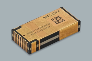
Regulatory Vicor 750W Non-Isolated Converter Unveiled
Vicor has launched the DCM3717 converter. The DCM3717 is a non-isolated converter operating from SELV input ranging from 40 to 60V, capable of regulating output voltage up to 10 to 13.5V. Based on an SM-ChiP package measuring 37×17×7.4mm, it delivers continuous power ratings of 750W and peak efficiency of 97%.
2020.05.21by 이수민 기자
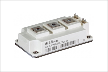
Infineon Announces Industry-Standard 62mm Package SiC MOSFETs
Infineon has added a 62mm industry-standard package to its CoolSiC MOSFET 1200V module product family. Unlike conventional 62mm IGBT modules manufactured from silicon, the CoolSiC 62mm modules made from silicon carbide can be used in applications such as photovoltaic, server, energy storage, EV charging, traction, commercial induction cooking, and power conversion systems.
2020.07.16by 명세환 기자

Intel Unveils Next-Generation 'Core Ultra Series 3' and vPro Platform for Enterprise PCs
Intel has officially unveiled the "Intel Core Ultra Series 3" for next-generation enterprise PCs and the latest vPro platform, addressing a wide range of demands from enterprise notebooks to high-performance workstations.
2026.03.26by 배종인 기자

ROHM Launches ESD Protection Diode Compatible with High-Speed Interfaces of 10Gbps or Higher
Semiconductor specialist ROHM has developed the 'RESDxVx series' of ESD (electrostatic discharge) protection diodes capable of responding to next-generation high-speed data communication environments exceeding 10Gbps, simultaneously enhancing both signal quality maintenance required in high-speed interfaces and IC protection performance.
2026.03.26by 배종인 기자











