


SK Hynix Develops 176-Layer 4D NAND Flash, Expected for Release Next Year
 Published2020.12.08 09:55
Reduced cell height and increased bit productivity by more than 35%
Plans to launch products for each application from mid-2021
SK Hynix has also joined the NAND flash stacking competition that Micron has ignited.
SK Hynix announced on the 7th that it has developed a 176-layer 512Gb (gigabit) TLC (Triple Level Cell) 4D NAND flash memory. SK Hynix provided samples of this product to a controller manufacturer last month to develop solutions.
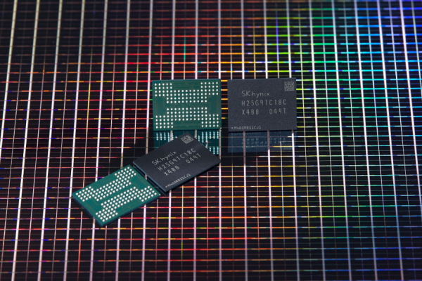
SK Hynix is introducing 4D products to the market that combine △CTF (Charge Trap Flash) technology, which reduces cell-to-cell interference by storing charges in insulators, and △PUC (Peri Under Cell) technology, which increases production efficiency by placing peripheral circuits at the bottom of the cell circuits, starting with 96-layer NAND flash.
SK Hynix officials explained that the 176-layer NAND developed this time is a third-generation 4D product, and that it has differentiated cost competitiveness with bit productivity improved by more than 35% compared to the previous generation.
By applying a new two-part cell area selection technology, the reading speed from the cell has been increased by 20% compared to the previous generation. We also applied technology that can increase speed without increasing the number of processes, achieving a data transmission speed of 1.6 Gbps, a 33% improvement.
SK Hynix plans to expand its market by application by sequentially launching consumer SSDs and enterprise SSDs, starting with a mobile solution product with a maximum read speed improved by approximately 70% and a maximum write speed improved by approximately 35% in mid-2021.
As the number of layers in NAND flash increases, cell distribution deterioration occurs due to a decrease in current inside the cell, interlayer distortion, and stack misalignment.
An SK Hynix official explained that this was overcome through ▲cell layer height reduction technology ▲layer-by-layer variation timing control technology ▲precision alignment correction technology.
In addition, the company plans to continuously develop 1Tb (terabit) products with double the capacity based on 176-layer 4D NAND to enhance the competitiveness of its NAND flash business.
Micron announced in November that it had begun mass-producing 176-layer NAND flash memory to customers. Industry sources believe the product is comprised of two stacked 88-layer NAND flash chips, rather than a 176-layer stack, but Micron denies this.
Meanwhile, market research firm Omdia predicted that the NAND flash market, which was 431.8 billion GB in 2020, will expand to 1,366.2 billion GB in 2024, growing at an average annual rate of 33.4%.
Comments
Related news

SK Hynix achieves KRW 1.3 trillion in operating profit, up 175% year-over-year.
SK Hynix explained that in the third quarter, mobile memory demand showed signs of recovery, but server DRAM and SSD demand for data centers remained weak, and as the memory market price trend shifted to a downward trajectory, third quarter revenue and operating profit each declined 6% and 33% compared to the previous quarter. Despite weak demand from server customers, DRAM shipments increased 4% compared to the previous quarter as a result of actively responding to new mobile and graphics demand and expanded consumer demand in certain sectors, but average selling prices fell 7% due to weak pricing trends in server DRAM and other products. NAND flash shipments increased 9% compared to the previous quarter driven by expanded sales of mobile products and new gaming console SSDs, but average selling prices declined 10% due to weak pricing in server products.
2020.11.04by 김동우 기자
.jpg)
WD Launches 3 New NVMe SSDs… Supports Architecture Extensions
WD unveiled three new NVMe SSD solutions at the online '2020 Flash Memory Summit' and announced the expansion of next-generation data-centric storage architecture. The three solutions were created based on Western Digital's unique vertical integration capabilities, spanning from NAND flash design and manufacturing to in-house SSD controller and firmware development. Through this announcement, WD plans to accelerate storage innovation for global customers ranging from cloud to OEM, enterprise, channel, and end-user sales markets, while continuing to support new system architectures, applications, and use cases.
2020.11.10by 김동우 기자
Xilinx and Samsung Electronics Launch the Industry's First Smart SSD
Xilinx showcased the SmartSSD CSD and partner solutions at the Flash Memory Summit virtual conference and expo. The product is a flexibly programmable storage platform implemented on an FPGA basis, enabling developers to address a wide range of data center challenges. Additionally, new types of software developers can easily implement innovative hardware-accelerated solutions using familiar high-level languages.
2020.11.11by 강정규 기자

Intel Unveils Next-Generation 'Core Ultra Series 3' and vPro Platform for Enterprise PCs
Intel has officially unveiled the "Intel Core Ultra Series 3" for next-generation enterprise PCs and the latest vPro platform, addressing a wide range of demands from enterprise notebooks to high-performance workstations.
2026.03.26by 배종인 기자

ROHM Launches ESD Protection Diode Compatible with High-Speed Interfaces of 10Gbps or Higher
Semiconductor specialist ROHM has developed the 'RESDxVx series' of ESD (electrostatic discharge) protection diodes capable of responding to next-generation high-speed data communication environments exceeding 10Gbps, simultaneously enhancing both signal quality maintenance required in high-speed interfaces and IC protection performance.
2026.03.26by 배종인 기자











