



Ultra-fine device manufacturing process, atomic layer deposition, lowers costs.
 Published2021.03.24 16:54
Success in fabricating ultra-fine semiconductor electrode patterns
Easy to manufacture, no need for expensive beam process
Semiconductor chips contain up to billions of transistors and diodes. These microscopic elements exist as patterns drawn into multiple layers of material. However, manufacturing these patterns requires an expensive process of drawing the shape with a beam.
Accordingly, a research team led by Professor Namgung Seon of the Department of Physics at Ulsan National Institute of Science and Technology (UNIST) announced on the 24th that, in collaboration with a research team from the University of Minnesota, they have developed a technology to manufacture semiconductor patterns using only atomic layer deposition, a process that involves layering materials thinly multiple times. This research was published online in the nanomaterials journal ACS Nano on February 24th and is awaiting official publication.
Atomic layer deposition is simpler and cheaper than beam-based techniques, and the channel width, which is the spacing between electrodes, can be changed to nanometers by depositing the number of atomic layers. It is also advantageous for the production of new concept semiconductor devices using two-dimensional semiconductor materials instead of silicon.
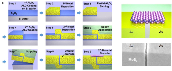
(Right) Using molybdenum disulfide, a two-dimensional material
The fabricated transistor [Image = UNIST]
Using the technology developed by the joint research team, they created ultra-fine "semiconductor electrodes" with channels of less than 10 nanometers and a two-dimensional transistor. They deposited electrodes, insulators, and electrodes in that order onto a substrate to create a nano-gap pattern. When this was peeled off the substrate and flipped over, an electrode pattern was completed with the distance between the electrodes being equal to the thickness of the insulating layer. The electrode surfaces were immediately separated from the substrate, resulting in a smooth surface, making them suitable for stacking two-dimensional semiconductor materials on top of the electrodes to create devices.
The joint research team also applied this to a transistor-based photodetector. The strong electric field between the ultra-fine transistor electrodes effectively separated the charged particles generated by light, enhancing detection performance. A photodetector is a device that detects light in the form of an electric current.
Professor Namgung Seon said about this technology, “It is a technology that mass-produces uniform nanometer-scale electrode structures using the existing semiconductor process technology, atomic layer deposition,” and “It will be useful for miniaturizing semiconductor structures, developing ultra-small optical communication modules, and developing optical semiconductor chips.”
Comments
Related news
KERI develops technology and equipment for early analysis of SiC material crystal defects.
Silicon carbide (SiC) is gaining attention as a power semiconductor material that offers superior durability, versatility, and efficiency compared to silicon (Si). However, SiC material contains invisible internal crystal defects that can degrade the performance of semiconductor devices. In response, a research team led by Dr. Bang Wook and Dr. Na Moon-kyung at the Power Semiconductor Research Center of the Korea Electrotechnology Research Institute (KERI) has developed a technology to analyze and evaluate crystal defects in SiC material at an early stage.
2021.03.10by 이수민 기자

"SiC and GaN-based semiconductor market shows clear growth trend"
The utilization frequency of wide bandgap (WBG) semiconductors based on silicon carbide (SiC) and gallium nitride (GaN) materials is increasing, as they allow higher voltages compared to conventional silicon (Si)-based semiconductors and exhibit lower losses. Recently, ON Semiconductor expanded its WBG device product portfolio by launching a 650V SiC MOSFET, thereby providing improved efficiency in power ranges that previously had insufficient service coverage.
2021.03.13by 이수민 기자

Fab equipment boom returns, with double-digit growth expected through 2022.
SEMI stated that as demand for electronic products surges due to the widespread adoption of non-face-to-face trends following COVID-19, investment in fab equipment is expected to continue increasing. According to the latest fab outlook report, global semiconductor industry fab equipment investment grew 16% in 2020, and is projected to rise 15.5% in 2021 and 12% in 2022.
2021.03.22by 이수민 기자

Intel Unveils Next-Generation 'Core Ultra Series 3' and vPro Platform for Enterprise PCs
Intel has officially unveiled the "Intel Core Ultra Series 3" for next-generation enterprise PCs and the latest vPro platform, addressing a wide range of demands from enterprise notebooks to high-performance workstations.
2026.03.26by 배종인 기자

ROHM Launches ESD Protection Diode Compatible with High-Speed Interfaces of 10Gbps or Higher
Semiconductor specialist ROHM has developed the 'RESDxVx series' of ESD (electrostatic discharge) protection diodes capable of responding to next-generation high-speed data communication environments exceeding 10Gbps, simultaneously enhancing both signal quality maintenance required in high-speed interfaces and IC protection performance.
2026.03.26by 배종인 기자











