


Siemens EDA: "Memory rebound expected in Q4…will help optimize semiconductor production."
 Published2023.03.29 09:06
.jpg)
Joseph Sawicki, Senior Vice President of Siemens EDA
Demand from the automotive industry is on the rise, and semiconductors are expected to recover.
ML-based solutions reduce semiconductor production time.
As the semiconductor market struggles due to the global economic downturn, Siemens EDA has issued an optimistic outlook that the market will quickly recover.
Siemens Digital Industries Software (Siemens EDA division) held the 'Siemens EDA Forum 2023' at the Lotte Hotel in Jamsil on the 28th and held a press conference to announce three Siemens EDA solutions that respond to semiconductor industry trends and the digitalization and AI era trends.
Siemens EDA stated, "Although the global economic downturn is causing a semiconductor slump, rapid recovery and growth are expected, and the semiconductor market remains positive in the long term due to demand from cutting-edge industries such as automotive." They added, "EDA is seeing continued growth in demand driven by the design of high-performance system semiconductors for applications such as AI and autonomous driving. Building on our 40-plus years of partnerships with semiconductor companies, Siemens EDA will continue to provide customers with the practical, systemic value they desire."
Joseph Sawicki, senior vice president of IC EDA, cited the slump in the memory market as a major cause of the semiconductor downturn experienced in the global market late last year in his presentation. “The semiconductor market bottomed out late last year, with the non-memory sector growing by 12%, while the memory market saw a -17% slowdown,” he said.
However, based on IC market forecast data, despite the disruption caused by supply chain issues earlier this year, the company forecasts that PC and server shipments will return to growth in the fourth quarter, driving growth in the memory market as well. Vice President Joseph stated, "In the long term, the semiconductor market is expected to grow at an average annual rate of 7% through 2030. Logic and memory will recover particularly quickly around the fourth quarter."
The semiconductor rebound was attributed to the growth of advanced industrial systems. Advances in the automotive, electronics, and 5G communications industries have led to a rise in the share of semiconductors in electronic products, from 16% in 2012 to 25%. Furthermore, data traffic is more than doubling every year, providing data centers with growth opportunities for semiconductor companies. Furthermore, ASIC design is also expected to increase.
In particular, automotive semiconductor content is expected to reach $1,000 per vehicle by 2028, and the automotive semiconductor market is growing at an average annual rate of 11%. Vice President Joseph stated, "Siemens EDA maintains a cooperative relationship with automotive OEMs."
■ Introducing three specialized AI-based scaling methods
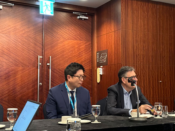
Semiconductor companies continue to invest despite low growth. Vice President Joseph said, "Despite the difficult fourth quarter of last year and the first quarter of this year, semiconductor companies around the world continued to invest heavily in R&D." For example, TSMC plans to hire approximately 6,000 new engineers to prepare for future manufacturing.
Siemens EDA claims that its machine learning (ML) solutions, which incorporate AI algorithms, can improve customer productivity.
Electronic Design Automation (EDA) is a software tool that automates the processes required for semiconductor design. It enables circuit design and error assessment and resolution through simulation. Siemens EDA acquired Mentor, solidifying its position as one of the top three EDA companies.
“EDA provides designers with a framework to verify chip designs, provides foundries with tools for production, and allows customers to focus on semiconductor production while optimizing software,” said Vice President Joseph.
Siemens EDA focuses its investments on three areas: technology scaling, design scaling, and system scaling.
The first is technology scaling. Supporting new nodes and 3D, Siemens EDA offers an integrated solution supporting 2.5D and 3D chiplet packaging. Siemens EDA stated that foundries will transition their computing systems for advanced nodes with curved masks and achieve cost savings by improving yields based on machine learning. Vice President Joseph noted, "It's currently uncertain whether this technique will be adopted beyond 2nm."
Next is design scaling, which supports maximizing the integration and utilization of all available transistors. Catafil synthesis tools accelerate AI IP creation, accelerate verification by eight times, cut design costs in half, and reduce SoC development time by up to 50%.
Finally, there's system scaling. Beyond chip verification, this approach offers a method for practically connecting ICs to systems on a stack. Running system software on SoCs is crucial for successful design, verification, and analysis. It supports the integration and verification of SoC functions within the system to ensure proper operation. For example, Pave360 and the Veloce system optimize performance from the silicon level to the entire system through digital twins during autonomous vehicle chip development.
“The three scaling approaches Siemens EDA focuses on are all interwoven into the value chain, complementing and reinforcing each other,” said Vice President Joseph.
Comments
Related news
196.9 billion won invested in research facilities and equipment, including semiconductors.
The government is investing 196.9 billion won this year to establish 19 new research and development infrastructure projects to support advanced industries such as semiconductors, displays, and batteries.
2023.03.22by 배종인 기자
.jpg)
U.S. Unveils Guardrail Draft… China Criticizes “Blatant Protectionism”
With the detailed regulations for the US semiconductor guardrails announced, the industry breathed a sigh of relief as it is anticipated that China will be able to expand production through equipment upgrades within the country. China raised its voice in criticism, stating that it undermines the international industrial network.
2023.03.23by 명세환 기자
Next to SiC·GaN is ‘Gallium Oxide’, “There’s a lot to eat”
In the midst of a paradigm shift toward compound semiconductors, referred to as next-generation semiconductors, movements to prepare the next step following SiC and GaN compound semiconductors have been detected.
2023.03.23by 명세환 기자
.jpg)
NVIDIA partners with ASML, TSMC, and Synopsys to manufacture next-generation chips.
As more transistors are packed onto advanced nodes and accuracy requirements become increasingly stringent, the computational time cost required for the most demanding workloads in semiconductor manufacturing has been outpacing Moore's law in recent years. Future nodes will demand even finer-grained calculations, but the available computational bandwidth provided by current platforms cannot accommodate all of them, resulting in a slowdown in the pace of semiconductor innovation.
2023.03.27by 명세환 기자
Developers looking for 'D2C' at affordable prices
Semiconductor manufacturers, which are typically B2B (Business-to-Business) enterprises, are adopting the D2C (Direct to Customer) distribution strategy that B2C (Business to Consumer) companies employ, and are gaining positive response from developer and engineer consumers.
2023.03.27by 명세환 기자











