



KLA-Tencor Launches Comprehensive Wafer Inspection and Review Product Family
 Published2016.07.12 10:06
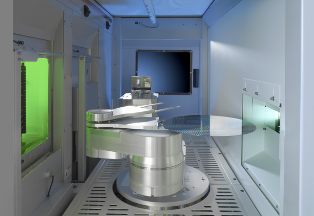
Ahead of SEMICON West, KLA-Tencor Corporation introduced the following six advanced wafer defect inspection and review systems for the manufacturing of advanced IC devices.
This includes the D30 (formerly called Gen 5) and D7 broadband plasma optical inspectors, Puma™ 6 laser scanning inspectors, CIRCL™5 all-surface inspection clusters, Surfscan SP5XP non-pattern wafer inspectors, and eDR7280 electron beam review and sorting equipment.
These systems employ various types of innovative technologies to implement comprehensive wafer inspection solutions, making it possible to detect and manage defects that have a significant impact on yield at every stage of IC manufacturing, from initial process characterization to production process monitoring.
Mike Kirk, Senior Vice President of KLA-Tencor’s Wafer Inspection business unit, said, “Through early collaboration with customers, we were able to gain a clearer understanding of inspection requirements for future process nodes. As a result, we were able to direct our R&D and engineering efforts to provide inspection systems and solutions that help customers resolve critical yield issues.”
In addition, “As an example, the D30 broadband plasma inspector not only provides impressive inspection performance (optical detection of sub-10nm defects) but also supports process debugging even for the most complex device designs.” “All systems included in our new wafer inspection product family combine innovative technologies that support advanced defect detection and monitoring, enabling customers to develop and secure state-of-the-art devices,” the company stated.
관련뉴스
KLA-Tencor Launches New Product for Advanced Semiconductor Packaging
2015.05.18by 명세환 기자
Silicon wafer shipments rise slightly after 6 months of sluggishness
The Semiconductor Equipment and Materials International (SEMI) announced through its quarterly silicon wafer industry report that global silicon wafer area shipments in the first quarter of 2016 increased compared to the fourth quarter of the previous year. First quarter silicon wafer area shipments totaled 2.538 billion square inches, representing a 1.3% increase from 2.504 billion square inches in the fourth quarter of the previous year, while declining 3.8% compared to the first quarter of the previous year (2.637 billion square inches).
2016.05.17by 명세환 기자

Intel Unveils Next-Generation 'Core Ultra Series 3' and vPro Platform for Enterprise PCs
Intel has officially unveiled the "Intel Core Ultra Series 3" for next-generation enterprise PCs and the latest vPro platform, addressing a wide range of demands from enterprise notebooks to high-performance workstations.
2026.03.26by 배종인 기자

ROHM Launches ESD Protection Diode Compatible with High-Speed Interfaces of 10Gbps or Higher
Semiconductor specialist ROHM has developed the 'RESDxVx series' of ESD (electrostatic discharge) protection diodes capable of responding to next-generation high-speed data communication environments exceeding 10Gbps, simultaneously enhancing both signal quality maintenance required in high-speed interfaces and IC protection performance.
2026.03.26by 배종인 기자

ST Launches 75V Drive IC Targeting 48V Industrial Motor Driving
ST Microelectronics has unveiled the 'STSPIN9P' series of 75V motor drive ICs tailored for 48V-class industrial drive system design. The new product family is characterized by half-bridge and full-bridge configurations that enable design scalability according to motor type and output conditions. Power supply circuits, protection functions, and current sensing circuits are integrated on-chip to simplify system configuration, and the devices are designed to support applications up to 500W maximum. The company plans to provide reference designs and demo boards to support development and evaluation in industrial automation, robotics, pumps, fans, lighting, and textile machinery.
2026.03.26by 배종인 기자











