


Increasing system efficiency and reducing losses by expanding IGBT performance
 Published2016.10.31 11:54
By Akhil Nair,
Technical Marketing Manager for IGBTs, ON Semiconductor
Insulated gate bipolar transistor (IGBT) devices are the key elements of high performance power conversion (HPPC) circuits. Power MOSFETs are generally used in medium and low power applications, while IGBTs with voltage ratings exceeding 1 kV are optimized for use in environments where voltage ratings exceeding 1 kV are required. Improving system efficiency and reducing losses using these devices is a major concern for engineers. This topic will be discussed in detail below.
Technologies such as gallium nitride (GaN) or silicon carbide (SiC) are too expensive. The unit price is too high for most applications in terms of cost reduction effects, and it remains a problem. In order to expect a price reduction for widespread use of this technology, economies of scale are required in addition to operational stabilization, so general commercialization of GaN/SiC technology is expected to take 5-8 years. Therefore, this method is not yet judged to have a high possibility of commercialization, and an alternative solution is urgently needed.
Therefore, rather than developing new materials, the semiconductor industry must find ways to improve the performance of existing IGBT technology. The question is, 'What should we do?'
Application Demand
High-power IGBT devices must be developed to support the increasing demand for higher frequencies, reaching at least 20 kHz for high-performance power conversion (HPPC) applications. This performance is expected to be applied in applications such as hybrid/electric vehicles (HEVs), solar infrastructure, uninterruptible power supply (UPS) devices, and HEV charging devices. These applications require significant power efficiency, especially at high frequencies (up to 95% in many cases). This means that the conversion losses of conventional IGBT technology must be reduced, depending on the application requirements.
Solving thermal issues is another important aspect of IGBT technology that should not be overlooked. In today's complex powertrain designs, space is often quite limited. By improving switching performance and system efficiency, the space required for heat sinking mechanisms can be minimized. This allows for greater board space utilization, reduced material costs, and improved reliability.
The only way to improve the performance characteristics of IGBTs while maintaining silicon technology is to take a new approach to IGBT design from various angles. There are two criteria that have the greatest impact on IGBT operation definition and power efficiency. The first is total switching loss (Ets), which is the sum of turn-on (Eon) and turn-off (Eoff) switching losses. IGBT switching losses are particularly critical when the device is operated at high switching frequencies and/or high operating temperatures.
The second is the conduction loss due to the Collector-Emitter Saturation Voltage (VCEsat). There is an inevitable trade-off between switching loss performance and conduction loss performance. Design engineers need to think about the whole rather than looking at the details in isolation, so they refer to the following figure of merit (FoM):
FoM= VCEsat x Ets
Figure of Merit (FoM) provides engineers with a consistent way to benchmark IGBT performance and compare devices manufactured by different vendors.
About IGBT switching losses
As described above, IGBT switching performance is basically composed of two factors: Eon and Eoff.
The Eoff of IGBT can be reduced in two ways:
a, by increasing the speed of the device... (i.e. reducing the transition time from high speed to low speed)
b, by blocking the tail current
Figure 1 below introduces two methods to reduce Eoff using the aforementioned methods. Here, we can see that the gray waveform increases sharply, which reduces Eoff by increasing the speed of the device (ultra-fast di/dt). This is not only bad in terms of EMI, but also causes the generated vibration to increase losses and cause additional losses in the device when the peak voltage exceeds the breakdown voltage. Therefore, an alternative method (green waveform) that allows for reduced losses while maintaining a natural and smooth turn-off is clearly preferable.
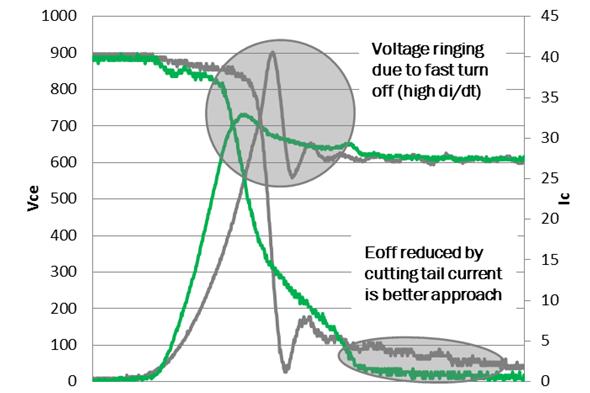
Figure 1 : Two approaches to reducing Eoff
Eoff is considered as an important measure of IGBT technology in most cases, but Eon is not given much meaning because it is operated by diodes co-packed together. Despite this fact, when considering the device as a whole and considering its impact on system performance, Eon is a factor that should never be overlooked because it has a significant impact on system loss. As shown in Figure 2, reducing the maximum reverse recovery current (IRRM) and reverse recovery time (TRR) improves the diode reverse recovery performance. Since a TRR value that is too low will result in ringing (a transient oscillation at the output caused by rapid changes in the input) and a very high dIRRM/dT value, the best way to reduce the reverse recovery loss (and by extension the Eon of the device) is to reduce the IRRM.
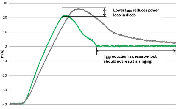
Figure 2 : Fast switching causing ringing
Limitations of IGBT Manufacturing
In fact, most IGBTs are designed as “vertical” devices, i.e., the emitter and gate terminals are formed on one side of the wafer substrate and the collector terminal on the other side. The FoM of a device is inversely proportional to the thickness of the wafer it is made of. That is, a thinner wafer can be used to achieve a higher FoM for an IGBT. Modern IGBTs are typically developed with wafers <200µm.
Fundamentally, the simplest way to improve the FoM of an IGBT is to reduce its thickness. However, using thin wafers is quite an adventure. Handling wafers as thin as a human hair is a major issue in the manufacturing process, but reducing the thickness to further lower the breakdown voltage is even more important.
Most modern IGBT technologies use field stop technology, which reduces thickness without changing the breakdown voltage. This technology utilizes a buffer layer (field stop layer) between the collector layer and the silicon, which not only allows for a higher breakdown voltage but also helps reduce the Eoff of the IGBT. Although a thick field stop layer is advantageous in terms of device performance, the silicon compression technology that must be used to compress it into one is not so simple.
Next generation IGBT solutions
ON Semiconductor has introduced a series of 1200 V IGBTs with ultra-high FoM using its own UltraField Stop (UFS) trench technology. The reference 1200 V/40 A device with UFS technology boasts 40% lower ETS and 15% lower VCEsat than most of the devices currently dominating the market. This means that these devices are high-performance products that reduce system energy loss and increase power efficiency.
UFS devices are mounted on SIO (silicon on insulator) surface. UFS is also the first product to use 105 µm thick wafers for 1200V IGBTs. Of course, ultra-fine devices require thicker field stop layers. By using thick field stop layers and thin wafers, these devices exhibit excellent FoM.
Another contributor to the performance improvement of these devices is the high-performance platinum-silicon-based diode co-packaged with the IGBT elements, which is specifically optimized to operate in conjunction with the UFS technology. This enables the desired reduction in reverse recovery losses without ringing. Figure 3 shows the power loss difference in a standard half-bridge inverter between the industry standard FS2 technology and ON Semiconductor’s UFS devices. Detailed application conditions for each measurement item are shown in the figure. Demonstrates how power loss is reduced through UFS technology.
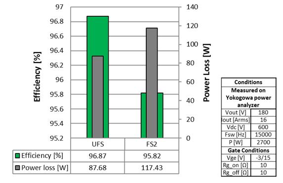
Figure 3 : Improved efficiency and power loss using UFS technology
With GaN or SiC adoption and commercialization still a few years away, power IC manufacturers must provide high-voltage switching devices based on silicon processes to the application market, and IGBT technology is expected to be a major driving force. Along with advances in fast-recovery diode technology, new IGBT technologies such as UFS are evolving power efficiency to meet future application demands.
관련뉴스

ON Semiconductor Completes Acquisition of Fairchild, Birth of 'Another Dinosaur Semiconductor Company'
온세미컨덕터와 페어차일드 세미컨덕터 인터내셔널은 온세미컨덕터가 현금 24억달러에 페어차일드를 인수하는 작업이 예정한 바와 같이 성공적으로 완료되었다고 공동 발표했다. 온세미컨덕터의 키스 잭슨 (Keith Jackson) 회장은 "페어차일드의 인수는 광범위한 애플리케이션 및 완성품 시장을 위한 전력 관리 및 아날로그 반도체 솔루션의 최고 공급 업체를 지향하는 당사의 비전을 한 단계 앞당겨줄 것이다. 페어차일드의 인수는 새로 재편되어가는 반도체 업계에서 수익성을 크게 확대할 플랫폼을 제공한다. 페어차일드의 제품군이 당사에 추가됨에 따라 업계를 선도하는 당사의 재정 상태가 한층 더 개선되었다. 또한 양사의 통합을 통해 더욱 주식 가치를 창출 할 수 있는 입지도 확보하게 되었다”고 말했다.
2016.09.23by 신윤오 기자
ON Semiconductor Launches Next-Generation Fan Motor Driver Series
온세미컨덕터가 180도 정현파를 통한 드라이빙 3 상 BLDC 모터용 소자 시리즈를 발표했다. 냉장고와 같은 가전 제품을 비롯해 게임 콘솔, 컴퓨터 기기 등의 냉각 팬에 사용하기 위해 설계된 LV8811, LV8813 및 LV8814 는 각각 3.6 볼트(V) 에서 16V의 전압 범위, 6에서 16V의 전압 범위를 갖고 있다. 이번에 출시된 고집적 ‘소프트웨어가 필요 없는’ 모터 드라이버 신제품들은 소프트웨어 개발 시간을 줄이며 모터 컨트롤 회로 설계를 단순화시켜준다. 또한, 이 소자들은 음향 잡음과 진동을 줄이고 에너지 효율 모터 컨트롤의 개발을 가능하게 한다. 이 소자들은 시스템 비용을 줄여주는 단일 홀 센서로 제어된다. 모터 스피드는 PWM 신호나 DC 전압으로 설정되며 리드 각도 쉽게 조종이 가능하다.
2016.09.29by 신윤오 기자
ON Semiconductor Launches Intelligent Charge Controller for Next-Generation Lithium-Ion Battery Development
온세미컨덕터가 차세대 리튬 이온 배터리 전력 제품 개발을 위한 고집적 싱글칩 파워 뱅크 솔루션을 출시했다. LC709501F 토탈 리튬 이온 배터리 솔루션은 간단한 FET 선택을 통해 최대 30 와트(W)까지의 최대 충전/방전 용량을 제공할 뿐 아니라 5V, 9V 및 12V의 넓은 전력 및 전압/전류 출력 작동 범위도 제공한다.
2016.10.19by 신윤오 기자

Intel Unveils Next-Generation 'Core Ultra Series 3' and vPro Platform for Enterprise PCs
인텔이 차세대 기업용 PC를 위한 ‘인텔 코어 Ultra 시리즈 3’와 최신 vPro 플랫폼을 공식 발표하며, 기업용 노트북부터 고성능 워크스테이션까지 폭넓은 수요 충족에 나섰다.
2026.03.26by 배종인 기자

ROHM Launches ESD Protection Diode Compatible with High-Speed Interfaces of 10Gbps or Higher
반도체 전문 기업 로옴(ROHM)이 10Gbps를 넘어서는 차세대 고속 데이터 통신 환경에 대응할 수 있는 ESD(정전기 방전) 보호 다이오드 ‘RESDxVx 시리즈’를 개발하며, 고속 인터페이스에서 요구되는 신호 품질 유지와 IC 보호 성능을 동시에 끌어올렸다.
2026.03.26by 배종인 기자











