



onsemi Launches High-Integration Sensing Products in Automotive Imaging Field
 Published2017.10.11 16:28

onsemi continues to advance its technology in the rapidly growing automotive imaging field with the introduction of two new high-integration 1.0 megapixel (Mp) CMOS image sensing products.
These devices provide a complete solution featuring image sensor and processing functions integrated into a low-power SoC that simplifies and accelerates adoption in applications such as rear and surround-view cameras.
Compared to conventional solutions consisting of discrete sensor and processor components, these devices enable over 30% superior PCB space savings, allowing designers to implement camera solutions without affecting vehicle styling or aesthetics.
The sensor represents one of several application areas supporting the advancement toward autonomous driving, and imaging devices such as the AS0140 and AS0142 are used in the ADAS field to enhance driver comfort, convenience, and safety.
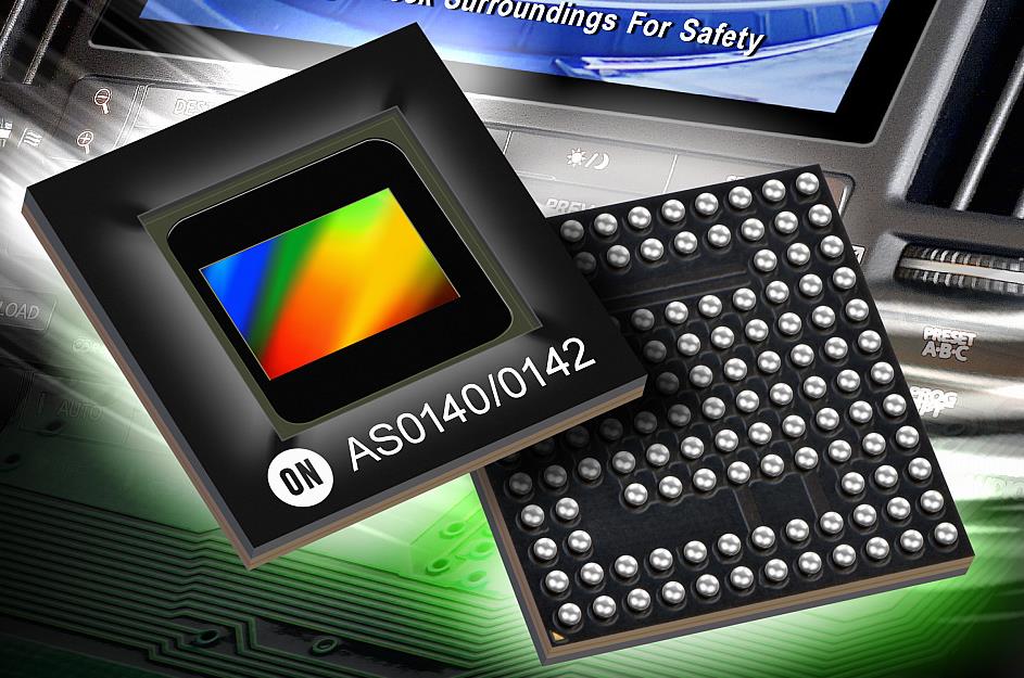
Both the AS0140 and AS0142 are 1/4-inch format devices capable of supporting 43 fps throughput at full resolution or 60 fps at 720p, featuring distortion correction, multi-color overlay, analog (NTSC) and digital (Ethernet) interfaces. Both SoC devices deliver enhanced image quality by employing adaptive local tone mapping (ALTM) to remove artifacts that adversely affect the acquisition process.
With a dynamic range of 93 decibels (dB), these new devices operate effectively in both high-sensitivity and low-sensitivity applications. As the number of cameras installed in vehicles continues to increase, the AS0140 and AS0142 provide automotive design engineers with the added-value feature of multi-camera synchronization support.
Ross Jatou, Vice President and General Manager of onsemi's Automotive Imaging Solutions division, noted, "These devices provide engineers with a complete SoC camera solution that combines low-power operation and high dynamic range while minimizing impacts related to PCB footprint and overall bill-of-materials cost," and added, "This means we can meet automotive manufacturers' imaging requirements both in terms of logistics and performance. Meanwhile, most existing solutions have relied on inefficient discrete device arrangements using separate image sensors and image processors, or have been SoCs with limited functionality."
Comments
Related news
ON Semiconductor Wins 'IoT Innovation Product Award' for IoT Development Kit
ON Semiconductor announced that its IoT Development Kit (IDK) has won the 2017 IoT Evolution Product of the Year Award. The IoT Evolution Product of the Year Award was presented by IoT Evolution magazine and IoT Evolution World, leading publications and websites in Internet of Things (IoT) technology. The IDK is a fully customizable platform that enables engineers to design differentiated IoT products and systems across diverse application areas including smart homes/buildings, smart cities, industrial automation, and mHealth.
2017.08.01by 신윤오 기자
ON Semiconductor Unveils Package Integrating RF SoC and BOM
ON Semiconductor has introduced a programmable RF System in Package (SiP) that integrates an advanced RF System-on-Chip (SoC) and a complete peripheral bill of materials (BOM) including a TCXO. The AX-SIP-SFEU is the most highly integrated Sigfox solution covering both uplink (transmit) and downlink (receive) communications. As the first product in a new SiP product family to be launched within several months, this device provides a variety of turnkey radio frequency (RF) solutions ready for immediate use to support applications requiring IoT connectivity.
2017.09.26by 김지혜 기자

ON Semiconductor CEO Selected as Most Respected Leader
ON Semiconductor announced that Keith Jackson, President and CEO, has been selected as one of the "Most Respected Leaders" by the Phoenix Business Journal. Since joining ON Semiconductor 14 years ago, Jackson has played a crucial role in driving operational excellence and industry-leading business practices. Thanks to this leadership, ON Semiconductor has created tremendous value that satisfies all stakeholders including customers, communities, employees, and shareholders. ON Semiconductor operates with a mission to deliver high-quality, energy-efficient solutions to address customers' electronic design challenges, grounded in world-class supply chain management and an ethical culture befitting global corporate social responsibility.
2017.09.29by 김지혜 기자

Intel Unveils Next-Generation 'Core Ultra Series 3' and vPro Platform for Enterprise PCs
Intel has officially unveiled the "Intel Core Ultra Series 3" for next-generation enterprise PCs and the latest vPro platform, addressing a wide range of demands from enterprise notebooks to high-performance workstations.
2026.03.26by 배종인 기자

ROHM Launches ESD Protection Diode Compatible with High-Speed Interfaces of 10Gbps or Higher
Semiconductor specialist ROHM has developed the 'RESDxVx series' of ESD (electrostatic discharge) protection diodes capable of responding to next-generation high-speed data communication environments exceeding 10Gbps, simultaneously enhancing both signal quality maintenance required in high-speed interfaces and IC protection performance.
2026.03.26by 배종인 기자











