갈륨나이트라이드(GaN) 소재는 실리콘(Si)이 가진 물리적 한계를 뛰어넘는다. GaN 화합물반도체가 대두됨에 따라 고온동작과 높은 전자밀도 및 항복전압의 특성을 이용해 고출력 RF 증폭기와 고전력용 반도체 소자 등으로 제품 상용화가 이뤄지고 있는 추세이다.
웨이비스, 차세대 0.2µm 공정 로드맵 공개
국방·수출규제 대응하는 제품 국산화 추진
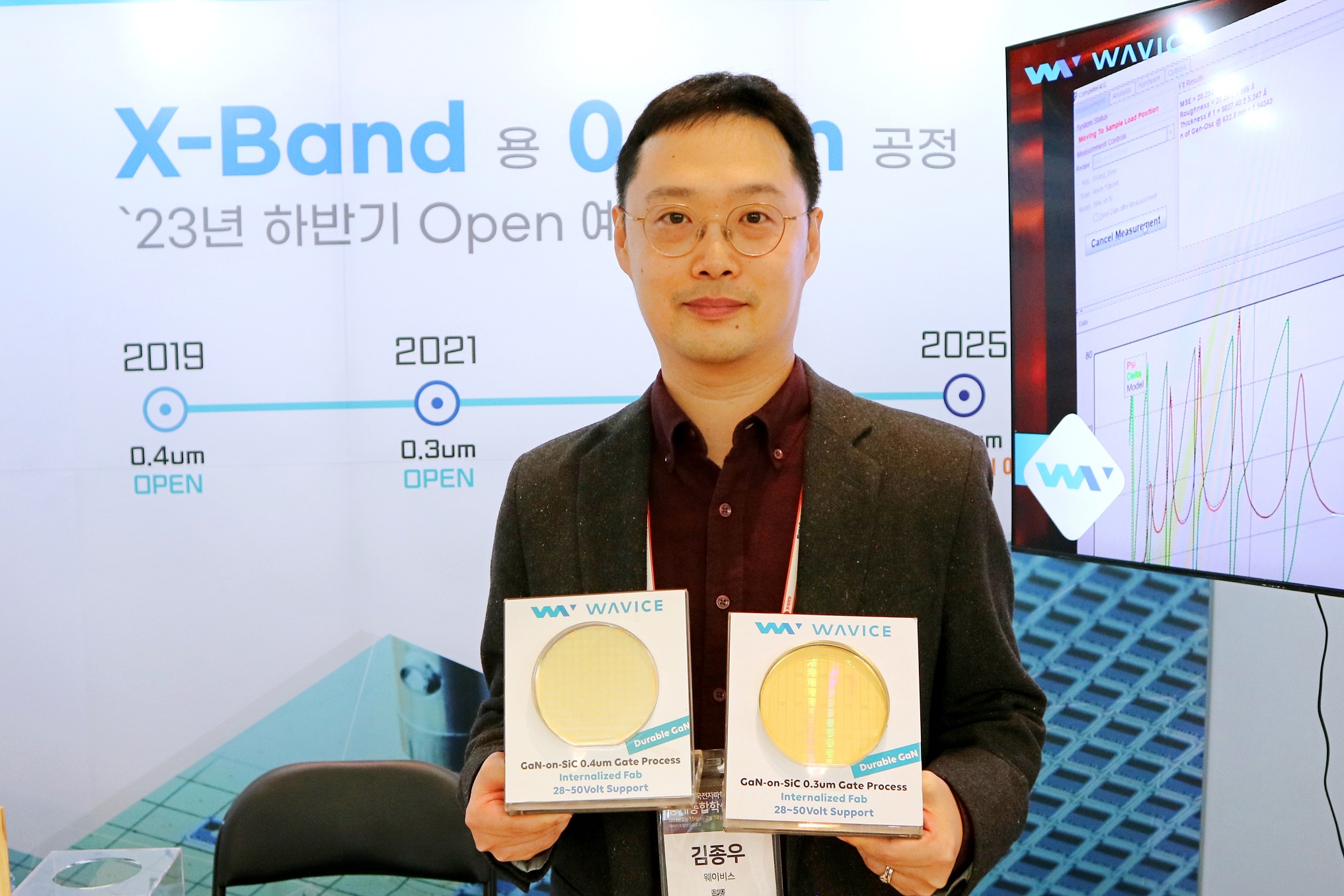
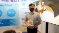
▲김종우 웨이비스 이사
갈륨나이트라이드(GaN) 소재는 실리콘(Si)이 가진 물리적 한계를 뛰어넘는다. GaN 화합물반도체가 대두됨에 따라 고온동작과 높은 전자밀도 및 항복전압의 특성을 이용해 고출력 RF 증폭기와 고전력용 반도체 소자 등으로 제품 상용화가 이뤄지고 있는 추세이다.
최근 개최된 한국전자파학회 동계종합학술대회서 국내 유일 RF GaN 파운드리를 보유한 반도체 기업 웨이비스(Wavice)가 차세대 0.2µm 공정 로드맵을 공개했다.
김종우 웨이비스 이사는 “2023년 하반기 X 밴드 대역을 커버하는 0.2µm 파운드리 서비스를 오픈할 예정이다”라고 밝혔다. X 밴드는 8∼12GHz의 SHF 주파수 대역을 말하며 파장이 짧아 △고해상도의 영상 정보 수집 △기상관측 △항공 △해상 관제 △군사용 레이더 등에 주로 사용된다.
.jpg)
▲웨이비스 RF GaN 파운드리 공정 로드맵
이에 김 이사는 “국방에 필요하고 수출 규제에 대응할 수 있는 제품들을 국산화해서 필요한 곳에 공급할 수 있도록 노력하겠다”고 말했다.
더불어 MPW(Multi-Porject Wafer) 서비스 신규 론칭해 고비용의 파운드리 서비스를 비교적 저렴하게 연구소 및 학교에서 이용할 수 있도록 하반기부터 제공할 예정이다. 김 이사는 “0.4 ~0.3 µm에서 연2회 MPW서비스를 제공할 예정이며 2024년 하반기부터 0.2 µm MPW도 이용 가능할 것”이라고 덧붙였다.
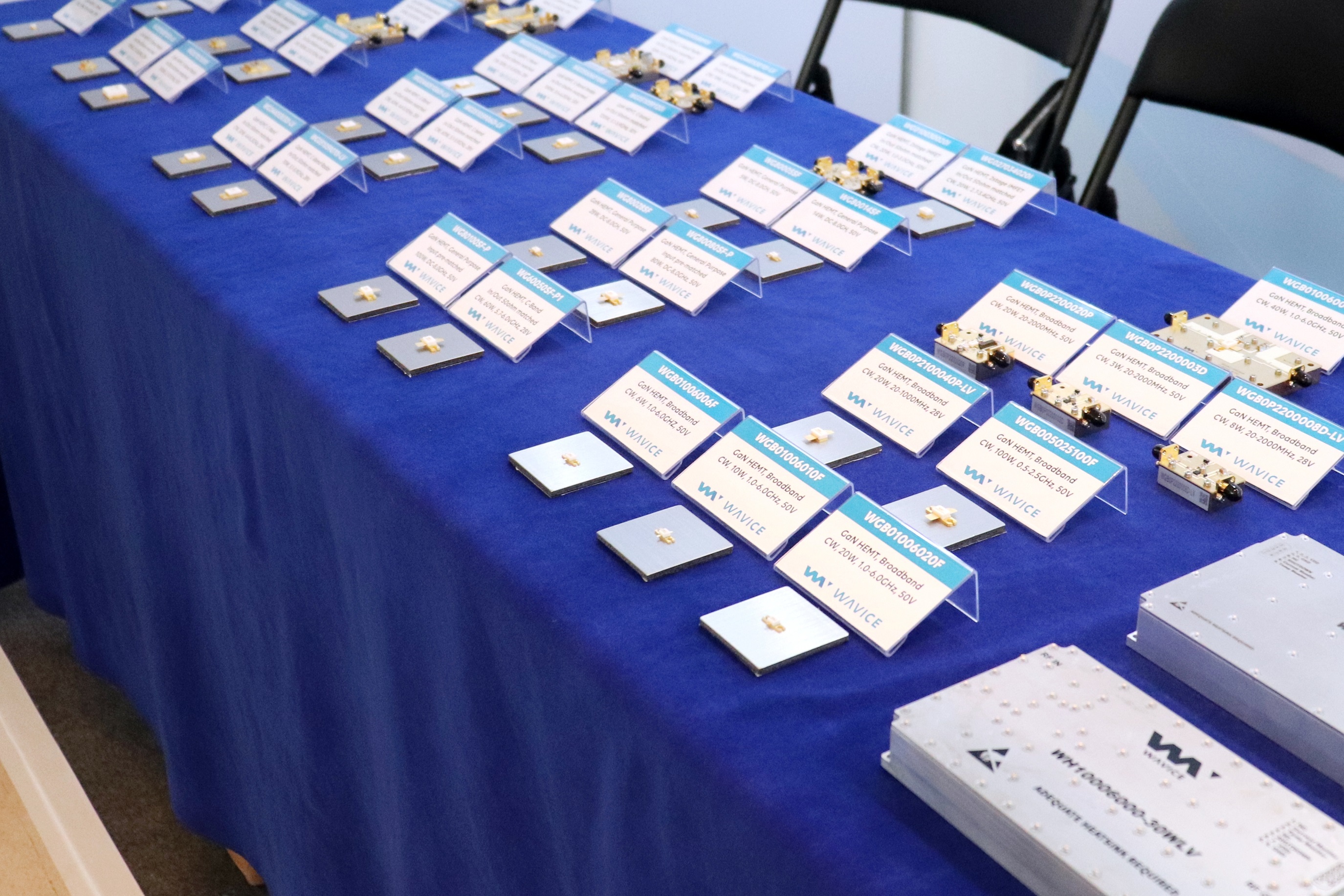
▲전시 부스에 공개된 제품 포트폴리오
한편, 웨이비스는 2017년 설립된 이후 차세대 전력반도체로 주목받는 GaN 반도체 개발에 집중하고 있으며, △항공·우주 및 국방 △네트워크 인프라 △ISM 및 방송 △RF 에너지 분야에서 포트폴리오를 가지고 있다.