


Institute for Basic Science Successfully Synthesizes 2D White Graphene "Path Opened to Commercialization of Rollable Displays"
 Published2019.05.23 09:52
| Successfully Elucidating the Mechanism of 2D Single-Crystal Synthesis
| Wide Opening of Rollable Display Commercialization
The Feng Ding Group Leader team (UNIST Distinguished Professor) at the Institute for Basic Science's Multidimensional Carbon Materials Research Unit announced on the 23rd that it has developed key technology for commercializing low-power, high-performance rollable displays that roll up like newspapers, in collaboration with research teams from China and Switzerland.
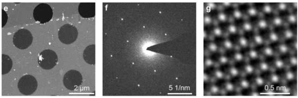
The research team has successfully manufactured single-crystal 2D white graphene at a large area of up to 100 cm², overcoming the previous limitation of manufacturing at only several square millimeters. This is a size that can be directly applied to semiconductor manufacturing processes.
2D white graphene (h-BN) is a 2D material with a thickness of 1-2 atomic layers in which boron (B) and nitrogen (N) atoms are arranged in a triangular form. Unlike graphene, it possesses insulating properties and can be applied as a 2D insulator.
The Ministry of Science and ICT and the Institute for Basic Science announced that the research results were published online in Nature (IF 41.577), the world's most prestigious academic journal, at 2 a.m. Korea time on May 23.
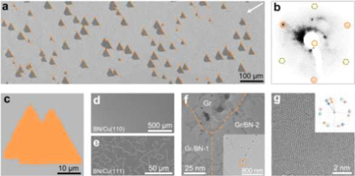
For the commercialization of rollable displays, thin and flexible 2D materials (1-2 atomic layers in thickness) are needed instead of rigid silicon, and when single crystals are used, device performance is also significantly enhanced.
Until now, apart from graphene, there have been no cases of manufacturing other 2D single-crystal materials at large areas suitable for commercialization.
Through simulation research, the research team discovered a synthesis formula showing that by using substrates with lower surface symmetry (symmetry being the number of identical shapes obtained when rotated 36 degrees) than the material to be synthesized, various 2D single-crystal materials can be grown at large areas.
Graphene, which has a hexagonal structure, is a material with 6-fold rotational symmetry showing the same shape every 6 degrees of rotation, while h-BN, which has a triangular structure, is a material with 3-fold rotational symmetry showing the same shape every 12 degrees
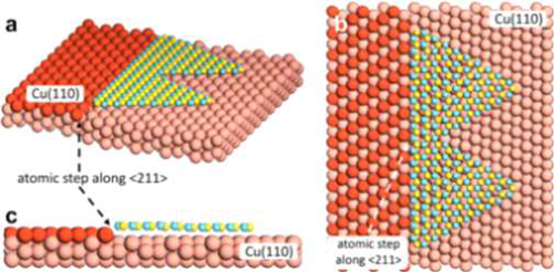
Based on this principle, the research team successfully manufactured 2D single-crystal white graphene insulator at a large area of 10 cm × 10 cm using a copper substrate with low surface symmetry.
Graphene alone, being a conductor, cannot implement semiconductors that turn on and off. However, by stacking conductor graphene and insulator white graphene layer by layer, it is possible to create thin, flexible next-generation high-performance, low-power semiconductors with only a few atomic layers in thickness without additional processing steps.
This research has opened a path to apply superior 2D materials, which were difficult to commercialize due to limitations in large-area manufacturing technology, to industrial applications.
White graphene is resistant to heat and can block radiation, and can be widely utilized not only in electronic devices but also in fields requiring light weight and thermal/chemical stability such as aircraft and spacecraft.
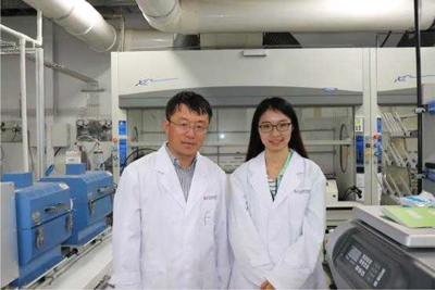
Feng Ding, Group Leader of the Institute for Basic Science, stated, "2D materials are excellent in themselves, but when multiple materials are stacked layer by layer and used together, they create synergistic effects. We have opened the door to the next-generation semiconductor market beyond silicon, and will contribute to implementing new material properties in electronic devices that we have never imagined before."
Related news
[KES 2018 Finding Hidden Technologies] Dream Factory "Graphene IoT Leakage Sensor"
If hazardous substances leak from equipment, property damage as well as human casualties can occur. Therefore, leaks must be detected in advance and appropriate countermeasures taken. Leak sensors must detect hazardous substances at the closest point, so durability is particularly critical. Dream Factory, located in Seongnam, Gyeonggi Province, manufactures sensors with improved sensitivity and accuracy through graphene nanomaterials secured via industry-academia-research collaborative research, and by applying them to monitoring systems, provides IoT leak sensors that can protect customers' personnel and assets.
2018.11.28by 이수민 기자
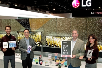
[CES 2019] LG Electronics Captivates CES with Rollable TV and HomeBrew
LG Electronics received a total of 132 CES Awards, including 19 awards selected by CTA, the organizer of CES, in November 2018, comprising the CES Best Innovation Award and CES Innovation Awards. In particular, the world's first rollable OLED TV unveiled by LG Electronics, the LG Signature OLED TV R, received the highest acclaim. Additionally, USA Today and other media outlets selected the LG HomeBrew capsule beer maker as the best product at CES.
2019.01.14by 이수민 기자
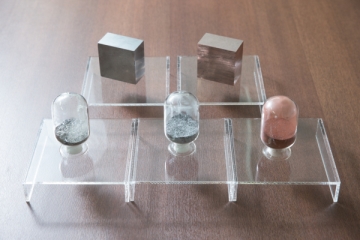
Saenggiwon develops a hybrid heat-dissipating material that doubles thermal conductivity by combining graphite powder.
The Korea Institute of Industrial Technology has developed a "metal hybrid thermal management material" that enhances thermal conductivity by 1.5 to 2 times by compositing graphite powder with metallic materials such as copper and aluminum, which are commonly used as thermal dissipation materials. As electronic components in electric vehicles, IT, and home appliances have recently become higher-performance, higher-power, more highly integrated, and miniaturized, operating temperatures are expected to rise from the current range of 120–200°C to as high as 400°C in the future, making the development of high-performance thermal management materials increasingly important. The thermal management material developed by the research team led by Dr. Oh Ik-hyun of the EV Component Materials Group has thermal conductivity of approximately 600 W/mK, which is 1.5 to 2 times higher than single materials such as copper (400 W/mK) and aluminum (220 W/mK), enabling rapid heat dissipation.
2019.05.20by 이수민 기자

Intel Unveils Next-Generation 'Core Ultra Series 3' and vPro Platform for Enterprise PCs
Intel has officially unveiled the "Intel Core Ultra Series 3" for next-generation enterprise PCs and the latest vPro platform, addressing a wide range of demands from enterprise notebooks to high-performance workstations.
2026.03.26by 배종인 기자

ROHM Launches ESD Protection Diode Compatible with High-Speed Interfaces of 10Gbps or Higher
Semiconductor specialist ROHM has developed the 'RESDxVx series' of ESD (electrostatic discharge) protection diodes capable of responding to next-generation high-speed data communication environments exceeding 10Gbps, simultaneously enhancing both signal quality maintenance required in high-speed interfaces and IC protection performance.
2026.03.26by 배종인 기자











