


ROHM Launches Bottom Electrode MOSFET 'RV4xxx Series'
 Published2019.07.30 11:11
| ON 저항 낮고 발열 저감 특징, SBD보다 소형
| 웨터블 플랭크 기술로 안정적 솔더 필렛 형성
ADAS에 꼭 필요한 차량용 카메라는 설치 면적이 제한되어 있어 탑재 부품의 소형화에 대한 요구가 높아지고 있다. 이러한 시장 요구에 대응하기 위해, 대전류를 유지함과 동시에 소형화를 실현할 수 있는 하면전극 패키지 MOSFET이 주목받고 있다.
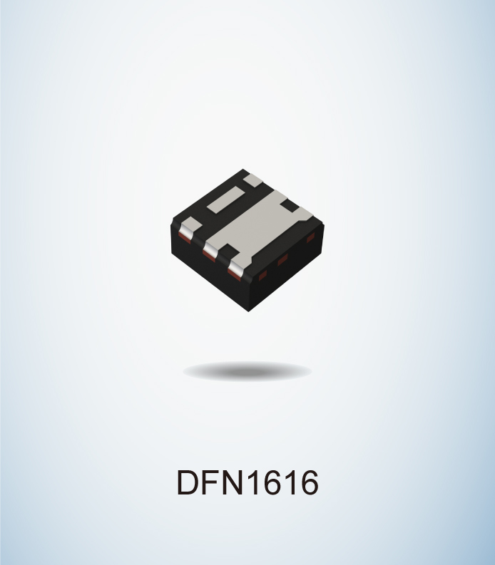
로옴은 부품 실장 후 신뢰성을 확보하는 1.6mm×1.6mm 사이즈의 MOSFET ‘RV4xxx 시리즈’를 개발했다고 23일 밝혔다.
기존 ADAS 카메라 모듈의 역접 보호 회로에서는 쇼트키 배리어 다이오드(Schottky Barried Diode; SBD)가 주류였다. 그러나 카메라가 점점 고해상도를 추구하면서 대전류화가 요구되는 자동차 전장 시장에서는 ON 저항이 낮아 발열을 저감할 수 있다는 특징에서 SBD보다 소형인 MOSFET로의 전환이 추진되고 있다.
예를 들어 전류 2.0A, 소비전력 0.6W일 경우, 자동차 전장 시장에서 많이 사용되고 있는 단자 타입 패키지의 MOSFET로 대체하면 SBD에 비해 30% 실장 면적을 줄일 수 있다.
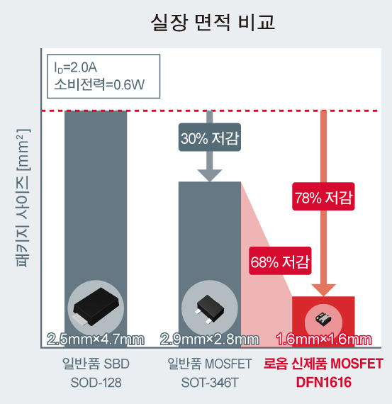

하면전극 패키지의 MOSFET의 경우, 하면이 전극이므로 방열성이 우수하여, 소형과 동시에 대전류화를 실현할 수 있다. 이에 따라 기존의 일반품 SBD 대비 78%, 일반품 MOSFET 대비 68%의 실장 면적을 저감할 수 있다.
RV4xxx 시리즈는 외관 검사에서도 이점을 갖는다. 외관 검사는 자동 광학 검사 및 AOI(Automated Optical Inspection)라고도 한다. 실장 기판을 카메라로 스캔하여, 부품의 결락 및 품질의 결함, 솔더링 상태 등을 검사하는 것이다.
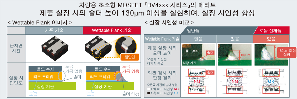
차량용 부품에서는 신뢰성 확보를 위해 부품 실장 후에 외관 검사가 실시되고 있다. 하지만 하면전극 패키지는 측면에 충분한 솔더 필렛(Solder Fillet)이 형성되지 않아, 자동차 전장이 필요로 하는 솔더 높이를 확보할 수 없다. 따라서 실장 후 솔더링 상태의 외관 검사가 어렵다는 과제가 있었다.
RV4xxx 시리즈는 자동차 전장의 신뢰성 규격 AEC-Q101에 따라 제작된 제품이다. 또한, 로옴의 독자적인 웨터블 플랭크(Wettable Flank) 형성 기술을 도입해 하면전극 패키지로도 안정된 솔더 필렛 형성이 가능하다.
.jpg)
웨터블 플랭크 형성 기술은 패키지 측면의 리드 프레임부를 절단하여 도금 가공을 실시한다. 그러나 리드 프레임을 절단할 때 발생하는 금속의 돌기 상태의 불필요한 부분은 절단면의 높이가 높아질수록 많이 발생한다.
불필요한 돌기 부분을 억제하기 위해 로옴은 리드 프레임 전면에 배리어 층을 구성하는 독자적인 공법을 개발했다. 이에 따라 부품 실장 시 제품이 기울어지거나 솔더에 불량이 발생하는 것을 방지할 수 있어 DFN1616 패키지(1.6mm×1.6mm)로써 패키지 측면의 전극 부분 높이 130μm 보증을 실현했다. 따라서 부품 실장 후의 외관 검사에서 솔더링 상태를 확실하게 확인할 수 있다.
로옴의 한 관계자는 “앞으로도 웨터블 플랭크 형성 기술을 활용하여 소형 패키지를 개발할 것”이라며, “MOSFET뿐만 아니라 바이폴라 트랜지스터 및 다이오드로의 전개를 추진하여 소형에 고신뢰성을 추구한 제품의 라인업을 확충해 나갈 것”이라고 밝혔다.

RV4xxx 시리즈는 5월부터 샘플 출하를 시작했으며, 올 9월부터 월 10만개의 생산 체제로 양산을 개시할 예정이다.
Comments
Related news

ROHM Develops Four Types of 1200V Withstand Voltage IGBTs for Automotive Compliant with AEC-Q101 Automotive Reliability Standard
The electrification of automobiles is accelerating. In conventional engine-equipped vehicles, the compressor is powered by the engine, but with the increase in electrified vehicles, the electrification of compressors is also being promoted. Additionally, vehicle heating has traditionally utilized engine heat, but demand is also increasing for systems that circulate hot water using PTC heaters as a heat source for heating. The semiconductors used in the inverter circuits and switching circuits of these applications have low switching frequencies, with IGBTs being the mainstream. Particularly in electric vehicles, the power consumption of compressors and heaters affects driving range, making high efficiency a requirement. In response, Rohm has newly developed four types of 1200V withstand voltage IGBT 'RGS Series' that comply with the automotive equipment reliability standard AEC-Q101.
2019.05.13by 이수민 기자
ROHM Launches Ultra-Low Power Boost/Buck DC/DC Converter for IoT
Rohm has developed the BD83070GWL, a MOSFET-integrated buck-boost DC/DC converter for mobile, wearable, and IoT applications. The BD83070GWL incorporates a low-loss MOSFET employing a power process 0.13µm BiCDMOS, achieving 97% power conversion efficiency at a load current of 200mA through a low-consumption current circuit. Equipped with Rohm's proprietary X Ramp PWM control technology, the device enables smooth buck-boost switching according to input voltage, with a quiescent current of only 2.8µA. Sample shipments of the new product commenced in April 2019, with mass production scheduled to begin in October 2019 at a production capacity of 1 million units per month.
2019.07.10by 이수민 기자
TI Launches Isolated Gate Driver for High-Voltage Systems with Integrated IGBT and SiC MOSFET Sensing
Texas Instruments announced new isolated gate drivers on the 18th that provide advanced monitoring and protection functions for high-voltage systems. Engineers can implement compact, efficient, and high-performance designs in traction inverters, onboard chargers, solar inverters, and motor drives using the UCC21710-Q1, UCC21732-Q1, and UCC21750. The newly released products are the industry's first to offer integrated sensing functions for both IGBTs and SiC MOSFETs. This simplifies design and improves system reliability in applications operating at up to 1.5kVRMS. Through integrated components, overcurrent conditions are rapidly detected and the system is safely shut down.
2019.07.18by 이수민 기자
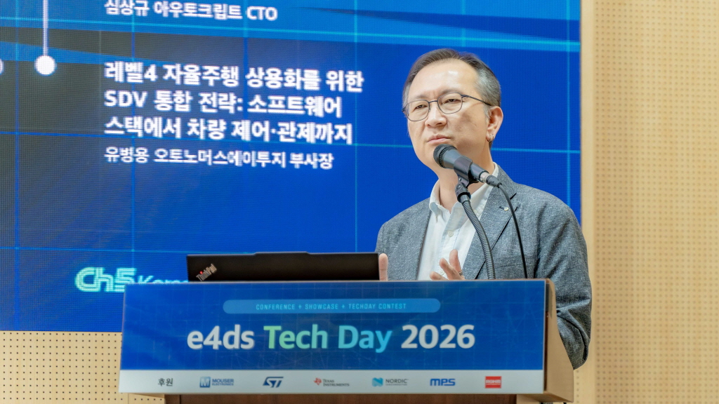
[e4ds Tech Day 2026 ⑨] Sim Sang-gyu, Autocrypt CTO: "In the Physical AI Era, Automotive Security Must Extend Beyond the Vehicle"
At e4ds Tech Day 2026, Sim Sang-gyu, CTO of Autocrypt, explained automotive cybersecurity strategies in the era of Physical AI and SDV (Software-Defined Vehicle). Automobiles are evolving as part of an ecosystem connected to AI, cloud, chargers, IoT, and robots, and he emphasized that the scope of security must expand beyond the vehicle interior to the entire connected environment. In particular, AI model tampering, adversarial attacks, OTA updates, and EV charger hacking were identified as major threats. He explained that response measures require zero trust, AI model integrity protection, intrusion detection, Security by Design and Default, and full lifecycle security management, and that proactive security system establishment beyond regulatory compliance is critical for securing future mobility competitiveness.
2026.10.12by 배종인 기자

Practical HIL Construction Strategy for Automotive and Off-Highway Controller Validation
As vehicle E/E architecture transitions to zonal structures and shifts to software-defined vehicles (SDV), the number of controllers (ECUs) requiring validation and software complexity are surging dramatically. Meanwhile, real vehicle testing cannot provide repeated verification under identical conditions and entails lead time and safety concerns. This white paper explains the principles of HIL (Hardware-in-the-Loop) validation and the structure of the NI platform composed of PXI, SLSC, and VeriStand, and through two actual implementation cases—Camera Record & Replay HIL for In-Cabin Monitoring Controller (ICMU) and Forklift Controller (VCU) HILS—describes how controller-level regression testing becomes possible. Additionally, it explicitly states application boundaries and limitations, such as lack of A2B support.
2026.10.12by 편집부











