


Samsung Electronics begins mass production of its 6th-generation V-NAND SSD, which breaks through 136 layers in one go.
 Published2019.08.06 17:52
Implementing a 6th-generation V-NAND 100-layer cell single-process
| Mass production of 512Gb 3-bit V-NAND planned this year
SSDs utilizing V-NAND, which can process more than 100 layers of cells at once, have entered commercialization.
Samsung Electronics announced on the 6th that it has mass-produced and supplied to global PC manufacturers an 'enterprise PC SSD' based on the 6th generation (1xx layer) 256Gb (gigabit) TLC (3-bit) V-NAND.
This product was manufactured using a single process (1 Etching Step) that pierces more than 100 cells at once, while simultaneously improving speed, productivity, and power-saving characteristics.
Samsung Electronics plans to launch products of various capacities and specifications, including 512Gb 3-bit V-NAND-based SSDs and eFUS, in the second half of this year to meet growing global customer demand, starting with mass production of 250GB SATA PC SSDs for businesses.
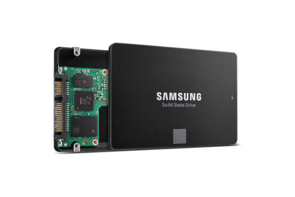
Samsung Electronics has mass-produced the 6th generation V-NAND, which has a density approximately 1.4 times higher than the 5th generation V-NAND, using 'Channel Hole Etching' technology.
The 6th generation V-NAND is electric By stacking 136 layers of molds and then simultaneously drilling tiny cylindrical holes to connect the cell structures, a 3D CTF cell with uniform characteristics was created.
In general, as the number of layers increases, it is difficult to maintain a uniform insulation state between layers, and the electron movement path also becomes longer, which increases NAND operation errors and causes a delay in data read time.
To overcome this, Samsung Electronics applied ‘ultra-high-speed design technology’ to the 6th generation V-NAND to achieve the fastest speed ever for a 3-bit V-NAND (data write time of 450 μs or less, read response latency of 45 μs or less), and reduced the operating voltage by more than 15% while increasing performance by more than 10% compared to the previous generation.
In addition, Samsung Electronics has achieved 256Gb capacity with less than 670 million channel holes in the 6th generation V-NAND, thereby reducing the number of processes and chip size compared to the 5th generation V-NAND (9x layers, approximately 930 million channel holes), and improving productivity by more than 20%.
The 6th generation V-NAND can produce next-generation V-NAND with over 300 layers in just three layers using a single process (1 etching step), which can further shorten the product development cycle.
Samsung Electronics plans to actively pursue a lead in the global mobile market by satisfying the ultra-fast and ultra-low power consumption characteristics required for next-generation flagship smartphones. In addition to leading the high-capacity market for next-generation enterprise servers, the company plans to continue expanding its 3D V-NAND business to the automotive market, which demands high reliability.
“By securing two generations of advanced 3D memory mass production technology, we have been able to launch a memory lineup with even higher speed and power efficiency at the right time,” said Kyung Kye-hyun, Vice President and Head of Solution Development at Samsung Electronics’ Memory Business Division. “We will further accelerate the development schedule for our next-generation lineup to rapidly expand the ultra-high-speed, ultra-high-capacity SSD market.”
Meanwhile, Samsung Electronics plans to expand its 6th generation V-NAND-based SSD lineup in earnest at its dedicated V-NAND line in Pyeongtaek starting in 2020.
Comments
Related news
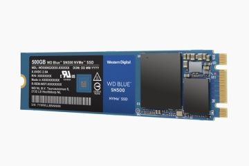
WD Launches WD Blue NVMe SSD Targeting Mainstream PC Users
Western Digital has added a new product, 'WD Blue SN500 NVMe SSD', to its WD Blue SSD portfolio. The newly introduced SN500 maintains the reliability characteristic of the WD Blue product line while delivering approximately three times higher performance compared to SATA products in the same lineup. Optimized for multitasking and resource-intensive applications, the product supports instant access to files and programs for content creators and PC enthusiasts. Based on Western Digital's proprietary 3D NAND technology, firmware, and controller, the 500GB model achieves maximum sequential read speeds of 1,700MB/s and sequential write speeds of 1,450MB/s, with low power consumption of approximately 2.7W.
2019.03.19by 이수민 기자
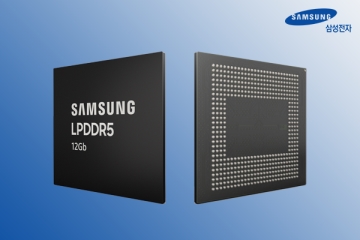
Samsung Electronics Begins Mass Production of 12Gb LPDDR5; Next-Generation 5G Smartphones Capable of Processing 44GB of Data in Just One Second
Samsung Electronics announced that it has become the first in the world to achieve mass production of 12Gb LPDDR5 mobile DRAM implementing the fastest speed ever in the 5G communication era. Starting from the end of this month, Samsung Electronics will secure the next-generation flagship smartphone memory market with 12GB LPDDR5 mobile DRAM packages equipped with eight second-generation 10-nanometer-class 12Gb chips, while responding swiftly to customers' demands for expanded supply. The 12Gb LPDDR5 mobile DRAM operates at 5,500Mb/s, approximately 1.3 times faster than the LPDDR4X currently mounted on high-end smartphones. When this chip is implemented in a 12GB package, it can process 44GB of data in just one second.
2019.07.22by 이수민 기자
Samsung Electronics Focuses on Expanding Sales of Key Products in Q2 Earnings Announcement
Samsung Electronics announced its second quarter 2019 consolidated results with revenue of 56.13 trillion won and operating profit of 6.6 trillion won. In the semiconductor business, demand recovered somewhat due to data center customers resuming purchases and increased mobile storage capacity, but overall business conditions remained weak and price declines continued due to inventory adjustments by major customers, resulting in lower performance. The display panel business improved overall results through one-time revenue generation in the small and medium-sized segment and expanded rigid product sales. In the IM business, smartphone sales volume increased due to expanded mid-to-low-end product sales, but profitability declined due to sluggish flagship product sales, intensified mid-to-low-end competition, and increased marketing costs.
2019.07.31by 이수민 기자

Intel Unveils Next-Generation 'Core Ultra Series 3' and vPro Platform for Enterprise PCs
Intel has officially unveiled the "Intel Core Ultra Series 3" for next-generation enterprise PCs and the latest vPro platform, addressing a wide range of demands from enterprise notebooks to high-performance workstations.
2026.03.26by 배종인 기자

ROHM Launches ESD Protection Diode Compatible with High-Speed Interfaces of 10Gbps or Higher
Semiconductor specialist ROHM has developed the 'RESDxVx series' of ESD (electrostatic discharge) protection diodes capable of responding to next-generation high-speed data communication environments exceeding 10Gbps, simultaneously enhancing both signal quality maintenance required in high-speed interfaces and IC protection performance.
2026.03.26by 배종인 기자











