


Lam Research Announces Additional Global Wafer Stress Management Solutions for 3D NAND Scaling
 Published2019.08.13 15:11
With the introduction of VECTOR® DT for backside deposition and EOS® GS wet etch for backside and bevel film removal, Lam Research expands its global wafer stress management product portfolio.
While high-aspect-ratio (HAR) deposition and etching are key technologies for 3D NAND scaling, increasing the number of deposition layers while controlling wafer bow due to stress accumulation in the stacked thin films has been a major challenge.
Wafer distortion caused by such stresses significantly affects wafer yield by reducing lithography depth-of-focus, degrading overlay performance, and causing structural deformation.
Improving overall yield requires careful management of stress at the wafer, die, and feature levels throughout the entire manufacturing process flow. In some cases, processes that could enhance performance are excluded due to their stress characteristics.
The VECTOR DT system, which provides an economical solution for controlling wafer bow in 3D NAND manufacturing, is the latest addition to Lam Research's plasma-enhanced chemical vapor deposition (PECVD) line.
VECTOR DT is a single-step solution that manages wafer shape by depositing a variable counter-stress film on the back of the wafer without touching the front side. This improves lithography results, reduces bow-induced defects, and enables high-performance, high-stress thin films.
In addition to counter-stress film deposition, Lam Research also offers backside film strip technology to enable customers to flexibly adjust wafer stress during 3D NAND manufacturing, and its EOS GS wet etch product complements the VECTOR DT.
Simultaneously removing backside and bevel films, it achieves industry-leading wet etch uniformity while completely protecting the front side of the wafer. Lam Research's EOS GS, part of its comprehensive wafer bow management solution, is also the product of choice for memory manufacturers worldwide.
“Our customers continue to significantly increase the number of memory cell layers, which can push cumulative stress and wafer bow beyond the limits of lithography equipment,” said Shesha Varadarajan, vice president of product management at Lam Research. “Minimizing stress-induced distortion is key to achieving target yields and realizing our cost-per-bit roadmap.”
“Lam Research is also expanding its stress management solutions to support customers’ vertical scaling roadmaps by adding the VECTOR DT and EOS GS systems to comprehensively manage stress,” he added.

Comments
Related news
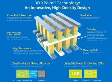
3D NAND on the Rise, Finding Processes and Materials to Solve Stacking Challenges
With 3D NAND supply volumes expected to surpass 2D NAND this year, interest is growing in the processes and materials required for stacking 3D NAND. On the 18th, the Semiconductor Electronic Materials Technology Conference (SMC, Strategic Materials Conference), hosted by the International Semiconductor Equipment and Materials Institute, was held under the theme "Scaling Challenges-The Future of Materials," discussing semiconductor material challenges for next-generation memory, market outlook for semiconductor materials, key process material technologies, and DRAM prospects. Sung-hyun Hong, Executive Director of Ram Research Korea, who presented, addressed the problems that arise as 3D NAND is stacked: "As the number of layers increases, the height becomes extremely high. If the structure is not harmonious, stress changes become severe. When stress becomes severe, the wafer bends, making handling difficult in subsequent processes."
2017.05.22by 김지혜 기자
Global semiconductor equipment shipments in Q1 2019 fell 8% compared to the previous quarter
SEMI announced on the 3rd that global semiconductor manufacturing equipment shipments in the first quarter of 2019 fell approximately 8% from the previous quarter to $13.79 billion. This represents approximately a 19% decline compared to the first quarter of 2018 shipments of $16.99 billion. In the Korean market, semiconductor manufacturing equipment shipments in the first quarter of 2019 fell 8% from the previous quarter to $2.89 billion, and decreased approximately 54% compared to the same period last year.
2019.06.04by 이수민 기자
Global Semiconductor Equipment Market to Snag This Year but Gain Momentum Next Year
SEMI forecasted that the global semiconductor equipment market revenue in 2019 would decline approximately 18.4% from $64.5 billion in 2018 to $52.7 billion. However, the global semiconductor equipment revenue in 2020 is expected to increase by 11.6% to $58.8 billion. This forecast reflects downward adjustments in investment due to regional political issues and market uncertainty. SEMI forecasted that the semiconductor equipment market would recover in 2020 due to rising memory consumption and China's semiconductor rise.
2019.07.11by 이수민 기자

Intel Unveils Next-Generation 'Core Ultra Series 3' and vPro Platform for Enterprise PCs
Intel has officially unveiled the "Intel Core Ultra Series 3" for next-generation enterprise PCs and the latest vPro platform, addressing a wide range of demands from enterprise notebooks to high-performance workstations.
2026.03.26by 배종인 기자

ROHM Launches ESD Protection Diode Compatible with High-Speed Interfaces of 10Gbps or Higher
Semiconductor specialist ROHM has developed the 'RESDxVx series' of ESD (electrostatic discharge) protection diodes capable of responding to next-generation high-speed data communication environments exceeding 10Gbps, simultaneously enhancing both signal quality maintenance required in high-speed interfaces and IC protection performance.
2026.03.26by 배종인 기자











