



Semiconductor Thin Film Deposition Process Now Observed in Real Time
 Published2019.09.18 14:41
| Real-time determination of thin film material concentration and crystal structure
| Used in semiconductors, OLED, batteries, electrode materials, etc.
Thin film deposition is one of the semiconductor processes that gradually deposits thin layers on a silicon wafer.
Thin films play a role in separating, connecting, and protecting semiconductor circuits. Therefore, semiconductor quality is improved when the thin film is formed as thinly and uniformly as possible.
However, since the thickness is less than 1 micrometer (㎛), implementing it is a process with high technical difficulty, and for this reason, it is important to measure and check the thin film formation status on a regular basis.
The Korea Institute of Industrial Technology (KITECH) has succeeded in developing a real-time deposition film measurement system for chemical vapor deposition materials that can observe, measure, and analyze the entire process of forming a thin film on a wafer inside chemical vapor deposition equipment in real time.
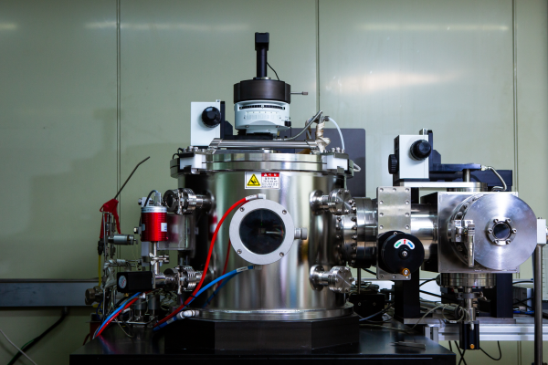
Chemical vapor deposition is a chemical deposition method that uses the chemical reaction of gases to deposit a thin film in the form of vapor, and is mainly used in semiconductor processes.
In the past, to check whether the thin film was properly deposited, the thin film had to be removed from the equipment and tested with a separate analysis device. However, in the process, the thin film could deteriorate due to contact with oxygen or moisture in the air, which could damage the reliability of the analysis results, and if a defect occurred in the thin film, it was difficult to determine the cause.
Dr. Heo Hoon's research team at the High Temperature Energy Systems Group of the Korea Institute of Science and Technology (KIST) solved this problem by installing an in-situ (=within a container) Raman spectroscopy device that can measure and analyze the deposition process of thin film materials inside chemical vapor deposition equipment.
The installed in-situ Raman spectroscopy device is based on the Raman effect, which occurs when monochromatic light is shined on a gas, transparent liquid, or solid, and light with a slightly different wavelength is generated in the scattered light.
By utilizing the Raman spectrum, which is a special arrangement of light generated by the Raman effect, various physical properties such as the concentration, crystal structure, and crystallinity of thin film materials can be identified in real time right inside the equipment. In addition, various variables such as compounds and reaction gases required for chemical deposition, and thin film growth temperature and time can be measured and analyzed to optimize the process.
The research team also developed an analysis technique that can infer permittivity based on the results of thin film material properties analysis. Permittivity refers to the degree to which an object becomes electrically charged when electrically charged molecules are aligned when an electric field is applied. The results of the dielectric constant analysis are used to develop semiconductor materials with low dielectric constant characteristics that are advantageous for high integration and high speed implementation.
The research team succeeded in depositing low-k semiconductor materials using the constructed system and analyzing the changes in physical properties according to the process and processing conditions in real time using Raman spectra, thereby increasing the possibility of developing new thin film materials.
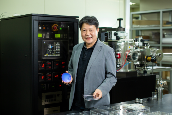
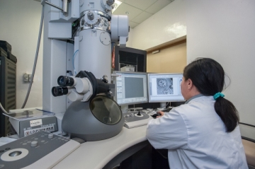
Holding a silicon wafer (Photo = Saenggiwon)
Dr. Heo Hoon said, “This is a case in which the limitations of the existing ex-situ (=outside the container) thin film analysis method were overcome with domestic technology, so it will be able to contribute to the localization of related materials and equipment,” and “It can be used in various fields such as not only semiconductors but also OLED materials, secondary batteries, or electrode materials for solar cells.”
Meanwhile, Saenggangwon is promoting the commercialization of a real-time deposition film measurement system together with semiconductor material companies.
Comments
Related news
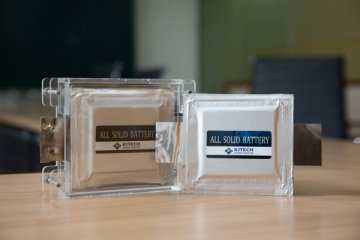
Domestic Researchers Successfully Develop Manufacturing Technology for 'All-Solid State Batteries' That Are Smaller and Safer Than Lithium-Ion Batteries
The Korea Institute of Industrial Technology has developed a manufacturing technology for all-solid-state batteries with a bipolar structure that can reduce the volume of battery packs while eliminating explosion and fire hazards. All-solid-state batteries refer to next-generation secondary batteries in which the electrolyte between the positive and negative electrodes inside the battery is changed from liquid to solid. Currently commercialized secondary batteries are lithium-ion batteries that use flammable liquid electrolytes, which carry a risk of explosion due to expansion when overheated or overcharged. The all-solid-state battery developed by the research team led by Dr. Kim Ho-sung, director of the Jeju Regional Headquarters of the Korea Institute of Industrial Technology, uses oxide-based solid electrolyte materials, making it safe with no explosion or fire hazards.
2019.06.18by 이수민 기자
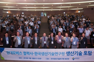
Saenggiwon to Begin Full-Scale Support for Technological Innovation for Large Corporate Partners
Korea Institute of Industrial Technology has stabilized quality by providing aluminum low-pressure casting technology support to Hyundai Mobis suppliers. Dr. Kim Dae-up's research team at KITECH's Jeonbuk Regional Headquarters identified process parameters capable of suppressing impurity generation during the aluminum low-pressure casting process and achieved quality stabilization by simultaneously performing flow analysis and defect analysis. This is the result of joint research conducted with Hyundai Mobis for 8 months through the Go-Together project. The Go-Together project is a program in which KITECH and major corporations jointly allocate R&D resources to support technological innovation for first, second, and third-tier suppliers. On the 10th, a production technology forum was also held between KITECH and Hyundai Mobis suppliers to advance identification of 2020 technology challenges and demands.
2019.07.12by 이수민 기자
Investment in raw materials, components, and equipment R&D will double starting next year.
In response to the weaponization of global materials strategy, such as Japan's export restrictions, the government is significantly expanding budgets for fundamental and original R&D in materials, parts, and equipment from a mid-to-long-term perspective. Following Japan's announcement of export restrictions on semiconductor core materials, the government has successively announced measures to strengthen competitiveness in materials and parts to break away from the external-dependency-type industrial structure through joint action by relevant ministries, as well as comprehensive R&D measures for materials, parts, and equipment to strengthen self-reliance capabilities in core original technologies. In line with this, the Ministry of Science and ICT is launching full-scale implementation of substantially expanded investment scale in fundamental and original R&D, innovation in R&D promotion methods to enhance investment efficiency and elimination of departmental silos, and expansion of R&D infrastructure based on openness, sharing, and cooperation.
2019.09.11by 이수민 기자

Intel Unveils Next-Generation 'Core Ultra Series 3' and vPro Platform for Enterprise PCs
Intel has officially unveiled the "Intel Core Ultra Series 3" for next-generation enterprise PCs and the latest vPro platform, addressing a wide range of demands from enterprise notebooks to high-performance workstations.
2026.03.26by 배종인 기자

ROHM Launches ESD Protection Diode Compatible with High-Speed Interfaces of 10Gbps or Higher
Semiconductor specialist ROHM has developed the 'RESDxVx series' of ESD (electrostatic discharge) protection diodes capable of responding to next-generation high-speed data communication environments exceeding 10Gbps, simultaneously enhancing both signal quality maintenance required in high-speed interfaces and IC protection performance.
2026.03.26by 배종인 기자











