


eGaN FET for LiDAR - Maximizing Laser Driver Performance Part 2
 Published2019.10.07 11:21
Over the past several years, a specific type of LiDAR known as ToF (Time-of-Flight) distance measurement has become widely used. When a laser is used as the optical source, it is possible to measure distances to small areas at remote distances. When used with adjustable optics, it is possible to measure the distance to a specific point and implement a three-dimensional map of an object.
EPC has developed the EPC9126 and EPC9126HC laser drivers to provide the performance of eGaN FETs to LiDAR systems and to enhance the technical level of LiDAR. Although the basic principle of this laser driver appears simple, parasitic components that many engineers overlook in design give it high-speed, high-voltage, and high-current characteristics.
This technical article was written to provide in-depth information on laser driver design so that users can maximize the use of the driver, and to answer commonly asked questions.
Help and Useful Information for the 9126
Following the previous article, let us review and move forward. Because the EPC9126xx is highly flexible, it can be used to try new ideas or to understand in detail the actual behavior of components for fast, high-current pulses. In this section, we would like to discuss additional recommendations for different approaches along with design details.
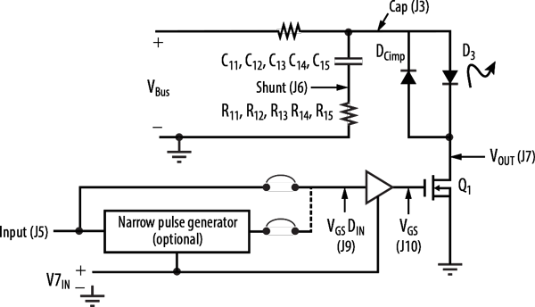
[Figure 12] is a block diagram of the EPC9126xx and provides a useful reference for this section.
Input and Output
The high speed of the laser pulse driver requires RF techniques, in particular the use of controlled impedance and standard 50Ω impedance for cables and measurements. If you are unsure what this means, there is a good reference1) to get started. It will be a good resource for those unfamiliar with this topic.
The input is terminated with a low-inductance 50Ω resistor (two 100Ω resistors connected in parallel) and is supplied directly to a comparator with a 2.5V threshold. Connecting a 50Ω cable and pulse generator results in minimal ringing and reflections.
If you want to drive this board directly with logic gates, keep in mind that the output impedance of many logic gates can be hundreds of ohms. This means that the input is not driven even with a sufficiently high voltage. In this case, you can remove the input terminating resistor, but the connection with the logic gate must be done in a way that minimizes all ringing and pulse reflections. If you are unfamiliar with it, refer to the reference mentioned above.
All outputs are designed to operate correctly with a 50Ω load. It is best to use a 50Ω cable connected to an oscilloscope with 50Ω internal input. If you set the scope input to 1MΩ and use external 50Ω termination on the scope input, it will work, but the bandwidth is limited by the typical input capacitance of the 1MΩ input connection. This capacitance limits the measurement bandwidth to <200MHz, which results in a minimum measurement rise time of about 1ns, which can appear much slower than actual operation.
Laser Mounting
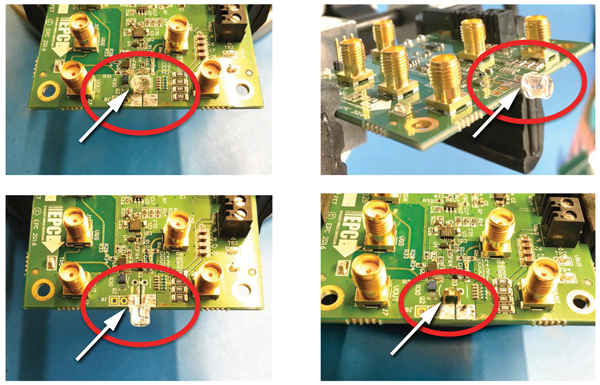
The EPC9126xx is designed to be flexible in the packaging and mounting of lasers or other loads. It has through-holes at 100mil spacing to mount soldered laser diode packages. It also provides footprints for surface-mount laser diodes from Excelitas.
Finally, it features bare pads that allow flexible mounting of other packages or bare laser diodes. [Figure 13] shows several ways to mount the laser.
Resonant Capacitor
With inductance minimized, the main parameters that the designer can control are voltage and resonant capacitance. The resonant capacitor should be an NPO/C0G ceramic dielectric or another capacitor with low loss, linearity, and stable dielectric such as ceramic, glass, or mica.
Charging Resistor
The resonant capacitor is charged through a charging resistor R1 (composed of a parallel combination of R2, R3, R5, R6 of the EPC9126xx) with a time constant τchrg given in (1).

Since t=5τchrg is required to charge the resonant capacitor to >99% of its final value, the maximum pulse repetition frequency can be set to PRF=1/5•τchrg. If the designer desires a higher PRF value, either allow the laser output to degrade slightly or reduce the R1 value. When R1 is reduced, additional current flows as Q1 turns on, but this can be acceptable if 5τchrg≫tw.
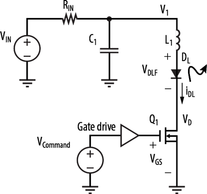
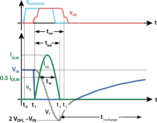
For the ideal resonant system shown in [Figure 5] and the related waveforms in [Figure 6], except for the initial charging of capacitor C1, the initial state of the capacitor becomes VC1(t2)=VIN–2VDFL. This is a very good approximation during recharging. All power is dissipated in R1, and the energy dissipated in R1 is as follows:

This is independent of R1, and the power dissipation is as follows:

At high PRF, power dissipation can be substantial and is added to the power dissipation of the laser itself. If the power dissipation is too large, other recharging methods such as a boost converter should be considered. This is outside the scope of this article and will not be discussed here.
Transmission Line Probes
All sensing measurement SMAs except shunt measurement use transmission line voltage probe principles to obtain waveform fidelity on a sub-ns time scale. These probes typically have relatively low probing impedances on the order of 500 to 5k, but this impedance is almost purely resistive, and the bandwidth can be very high, reaching several GHz.
Since the probe is embedded in the PCB and can be ideally connected to the node of interest, it improves waveform fidelity and repeatability. Another important consideration when measuring high voltages in a circuit is not to deviate from the measurement point. The basic principle of such probes is described in detail in 2).
Three characteristics must be considered to perform useful measurements with the embedded probe.
First, it must be connected to an oscilloscope with the scope input set to 50Ω. Using a 1MΩ input with a 50Ω terminator is not recommended as it severely limits the bandwidth of almost all scopes.
Second, each embedded probe has its own attenuation factor that must be considered.
Third, the low impedance of the probe means that significant power dissipation can occur at points where the average DC voltage, i.e., the drain voltage, is large.
To prevent this dissipation, high-voltage measurement test points include DC blocking capacitors. This forms a high-pass filter with minimal effect on the waveforms of general interest. However, if longer pulse widths are used, incorrect results can occur at these test points, so an external probe should be used.
The embedded transmission line probe has been verified to produce results almost identical to Tektronix's P9158 3GHz transmission line probe3), so the expected bandwidth is at least 3GHz.
Current Sensing
Current sensing is one of the most difficult issues in power electronics. Current sensing in a pulsed laser driver has both advantages and disadvantages. The advantages include operation verification, timing determination of laser pulses, and optical power control that maximizes range while ensuring eye safety.
However, current sensing also has many disadvantages. These include added inductance in the power loop, increased power loss, degraded waveform accuracy, cost burden, and reduced laser drive voltage to overcome inductance.
The current measurement function is included in the EPC9126xx in the form of a resistive current shunt composed of four 0402 resistors to minimize the added power loop inductance. These small resistors can be used at very high currents due to the low duty cycle of the laser driver.
There is a tendency to compromise current shunt performance to include economic current sensing while minimizing negative impacts on performance, which can result in significant distortion of the current waveform.
Generally, it is desirable to use a shunt with a very small resistance value to minimize the voltage drop due to high peak current. Unfortunately, even the very small inductance of five 0402-sized resistors connected in parallel can have a large effect on shunt impedance and the measurement itself.
This effect can be conservatively estimated by assuming a rectangular pulse with edge transition time tt=2ns. The pulse with maximum 3dB bandwidth can be calculated with the following equation:

The partial inductance contribution of the shunt, indicated as L1shunt, was estimated by replacing the laser diode with a flat copper plate on the PCB and using the oscillation frequency when switching of Q1 began. This yielded L1shunt=1.21nH.
The shunt resistor was then mounted in reverse to evaluate the inductance, and finally the shunt resistor was replaced with a copper plate and measured. These results are shown in [Table 2].

[Table 2] shows that compared to the case without a shunt, Lshunt,A=200pH for normally mounted shunt resistors and Lshunt,B=40pH for reverse-mounted shunt resistors. At fw=175MHz, the inductive reactance for Lshunt,A is as follows:

The resistance value of the shunt must be at least 5 times the inductive reactance, corresponding to Rshunt,A≥1.1Ω. As a result, a voltage drop of 39V occurs at the peak current, which reaches 40% of the transistor's rated voltage. By reverse-mounting the shunt resistor and reducing it up to 5 times, Rshunt,B≥0.22Ω can be obtained. The final value Rshunt=0.20Ω was selected based on component availability.
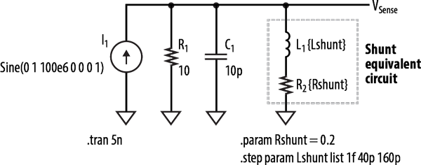
To verify the effect on the waveform, [Figure 14] shows a simple shunt simulation circuit performed with tw=3.3ns for the three cases mentioned above. [Figure 15] shows the results. Even with a small value of 200pH (0402 resistors connected in parallel on the PCB), it can be seen that significant errors can occur for short pulses.
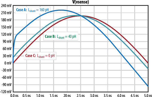
The effect of inductance is to differentiate part of the current signal, exaggerating the initial portion and peak of the waveform. As the pulse becomes shorter, this error becomes more severe.
Unfortunately, boards corresponding to Case A are being shipped because it is economically difficult to reverse-mount the resistors. With sufficient commercial incentive, such suppliers could be found. One manufacturer is already proceeding this way, but unfortunately the maximum value provided at the time this article was written is too small to measure.4)
If more accurate current measurement is required, the resistor must be remounted in reverse or a larger value is required, and both may be necessary. If the oscilloscope has programmable frequency and single-pole cutoff capabilities with low-pass filter functionality, the current shunt response with a pole at the same frequency should be zeroed out to cancel for more accurate results.
Dual Edge Control
As discussed, the resonant capacitive discharge laser driver has several useful characteristics. However, they have serious limitations for a given power loop inductance. That is, the pulse height can be controlled but the pulse width cannot. Also, pulse width can be used to control total pulse energy, and if such control is needed for individual pulses, it is easier to control than pulse amplitude.
In some cases, the laser diode or other load must be separated from the PCB. This requires a series of interconnections that can add significant inductance. To address some of these limitations, dual edge control is used, meaning both the turn-on and turn-off of the drive FET are used to control the pulse shape.
To use the EPC9126xx with dual edge control capability, you must first understand the limitations of the UCC27611 gate drive with a minimum pulse width of approximately 6ns, though not specified in the specifications. This limits pulse length.
For typical dual edge control applications, the resonant capacitor and charging resistor may need to be changed. If current needs to be limited, the charging resistor can be used for this purpose because there is additional bus capacitance at the bus voltage input of the PCB.
Finally, when the switch turns off, the current in the power loop inductance is cut off, which can cause ringing and overshoot on the FET and laser diode or other load. This ringing depends on the current of the inductance and turn-off time, as well as the capacitance of the laser, FET, and PCB.
To control voltage overshoot, some clamp diodes may need to be added. Finding a suitable clamp diode is very difficult. Most diodes have package inductance similar to power loop inductance, which limits response speed.
If the clamp current is high, a larger diode to handle it can have significant capacitance that causes additional ringing, and in some cases can cause unwanted laser pulses to be triggered repeatedly.
When using the EPC9126xx for dual edge applications, it is advisable to plan both careful simulation and experimentation. Experimentation is particularly important. Empirically, when selecting a diode with the required voltage and current ratings, currently available models do not accurately describe diode behavior for the very short transitions required in LiDAR applications.
Narrow Pulse Generator
Based on Jim Williams' traditional design approach, the EPC9126xx also includes a narrow pulse generator5). Basically, this circuit is not activated, and the pulse input goes directly to the gate drive IC. However, by changing the 0Ω jumper and using this circuit, very short pulses can be generated. If you want to use this circuit, it is recommended to refer to Williams' application note.
Conclusion
The performance of GaN power transistors can enhance the performance of laser drivers. The ability to generate high-current pulses in single-digit nanoseconds delivering hundreds of watts in just a few square millimeters is exceptionally outstanding. This is one of the key factors enabling economical high-performance LiDAR implementation based on compact form factors, which can further accelerate the LiDAR revolution.
References
1) H. Johnson and M. Graham, High-Speed Digital Design – A Handbook of Black Magic, Prentice Hall PTR, 1993.
2) J. Weber, Oscilloscope Probe Circuits, Tektronix Inc., 1969.
3) Tektronix Inc, "20X Low Capacitance Probe – P6158 Datasheet," 2017, (https://www.tek.com/sites/default/files/media/media/resources/P6158-Datasheet-60W120263_0.pdf)
4) Susumu 2018 Product Catalogue (EN), 2018-04-06, pp. 53-54. 2018, (https://www.susumu.co.jp/common/pdf/n_catalog_partition09_en.pdf?v=20180406)
5) J. Williams, "AN98 Signal Sources, Conditioners, and Power Circuitry – Circuits of the Fall, 2004: Nanosecond Pulse Width Generator," Linear Technology Corporation, 2004.
#Regarding this article, e4ds.com is conducting experimental discussions on GaN technology for LiDAR. If you have questions about this technology or would like to contribute additional articles, please leave a comment below.
Related news
.png)
KETI Localizes Autonomous Driving LiDAR Sensors for Unmanned Transport Robots
KETI has succeeded in localizing a scanning lidar sensor for SLAM used in autonomous navigation of smart factory autonomous mobile robots. In the past, AGVs operated using a traditional SLAM method that recognized artificial markings such as optical recognition metal wires or magnetic lines attached to the floor and traveled along predetermined paths. Recently, AGVs using autonomous navigation methods that recognize position using lidar without separate markings and further create and utilize surrounding maps have become commonplace. Until now, scanning lidar sensors for SLAM had to rely on Japanese and German products priced around 2 to 3 million won. The scanning lidar sensor for autonomous navigation of unmanned mobile robots developed by KETI this time is capable of 180° detection and can detect objects as small as 10cm at a maximum distance of 30m.
2019.08.26by 최인영 기자
eGaN FETs for LiDAR - Getting the Most Out of Laser Drivers Theory
Lidar is a form of radar that generates electromagnetic waves in a broad spectrum. Over the past several years, Time-of-Flight (TOF) distance measurement, one specific form of lidar, has been widely adopted. When a laser is used as the optical source, distance measurements can be taken even to small areas at far distances, and when used with adjustable optical devices, the distance to that point can be measured and a three-dimensional map of the object can be implemented.
2019.09.09by 명세환 기자
eGaN FET for Lidar - Maximizing Laser Driver Performance Part 1
Lidar is a form of radar that generates electromagnetic waves across a broad spectrum. Over the past several years, ToF (Time-of-Flight) distance measurement, a specific type of lidar, has been widely adopted. When a laser is used as the optical source, it enables distance measurement even to small sections at far distances. When used with adjustable optics, it can measure the distance to a specific point and implement a three-dimensional map of the object.
2019.09.25by 최인영 기자

Intel Unveils Next-Generation 'Core Ultra Series 3' and vPro Platform for Enterprise PCs
Intel has officially unveiled the "Intel Core Ultra Series 3" for next-generation enterprise PCs and the latest vPro platform, addressing a wide range of demands from enterprise notebooks to high-performance workstations.
2026.03.26by 배종인 기자

ROHM Launches ESD Protection Diode Compatible with High-Speed Interfaces of 10Gbps or Higher
Semiconductor specialist ROHM has developed the 'RESDxVx series' of ESD (electrostatic discharge) protection diodes capable of responding to next-generation high-speed data communication environments exceeding 10Gbps, simultaneously enhancing both signal quality maintenance required in high-speed interfaces and IC protection performance.
2026.03.26by 배종인 기자











