



Applied-BE Accelerates 'Chip Integration Technology' for Future Industries
 Published2020.11.04 10:23
Establishment of joint programs and COE between the two companies
Applied Materials announced on the 4th that it is collaborating with BE Semiconductor Industry (Besi) to develop a complete and proven equipment solution for die-based hybrid bonding.
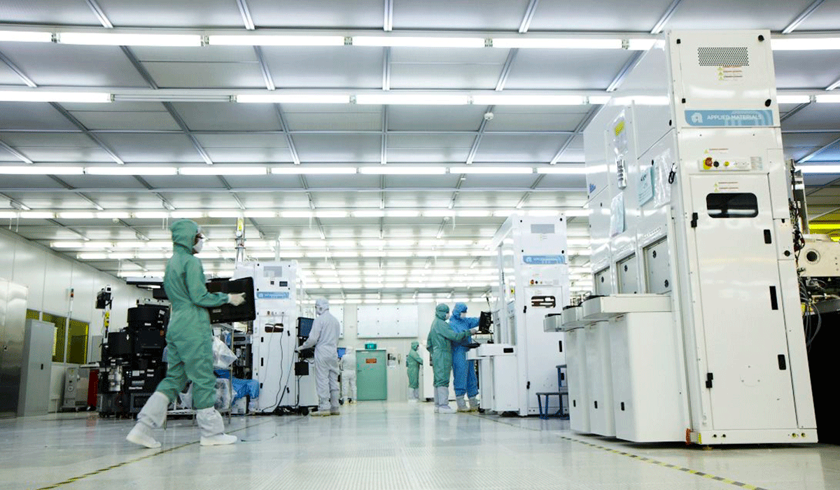
Die-based hybrid bonding is a new inter-chip connection technology that enables heterogeneous chip and subsystem design in products related to advanced technologies such as high-performance computing, artificial intelligence (AI), and 5G.
It connects multiple die-shaped 'chiplets' using direct copper interconnects. Through this technology, designers position chiplets of various process nodes and technologies closer together physically and electrically, providing performance equal to or better than that of a single large die.
Hybrid bonding improves overall performance, power, efficiency, and cost by increasing chip density and reducing interconnect wiring lengths between chiplets.
In addition, a complete die-based hybrid bonding equipment solution requires a wide range of semiconductor manufacturing technologies in addition to high-speed, ultra-precision chiplet placement technology. To this end, the joint development program between the two companies combines Applied Materials' expertise in etching, planarization, deposition, wafer cleaning, metrology, inspection, and particle defect control processes with Besi's die placement, interconnect, and assembly solutions.
As traditional 2D scaling slows down, the semiconductor industry is exploring heterogeneous design and chip integration as new ways to improve PPACt (Power, Performance, Space Cost, and Time to Market). To this end, the two companies established a Center of Excellence (COE) focused on next-generation chip bonding technology and created a joint development program.
Based on front-end and back-end expertise, this program provides customers with integrated hybrid bonding configurations and equipment solutions optimized for the entire process.
“We are pleased to combine the semiconductor industry’s leading materials engineering with advanced packaging technology,” said Besi CTO Ruert Boomsma. “The collaboration between the two companies will accelerate the adoption and expansion of hybrid bonding in advanced technology fields such as 5G, AI, high-performance computing, data storage, and automotive.”
Comments
Related news
Applied Materials Launches Mass Production Solutions for Three Next-Generation Memory Types: M-RAM, Re-RAM, and PC-RAM
In the AI and big data era, the memory sector requires innovations at the angstrom unit level, which is more precise than nanometers, and must address the following challenges. First, it is necessary to find ways to efficiently collect, process, store, and analyze vast amounts of data required for AI. Second, a computing architecture must be devised that can best implement the performance, power efficiency, and cost requirements of tens of billions of devices that constitute the IoT. Next, chips for machine learning and inference applications must be further optimized in cloud data centers and edge devices. Finally, a comprehensive understanding of solutions ranging from materials to systems must be established.
2019.09.09by 이수민 기자
Microchip Unveils SiC SBD Power Components to Boost EV Reliability
Microchip Technology has launched newly certified 700V and 1200V SiC Schottky Barrier Diode (SBD) power devices. The devices provide EV system developers with solutions that meet stringent automotive quality standards across a wide range of voltage, current, and package options. The AEC-Q101 certified devices maintain high quality while enabling EV power developers to maximize system stability and durability, and implement reliable and extended application lifespan. With superior avalanche performance, the devices reduce the need for external protection circuits, thereby decreasing system cost and complexity.
2020.10.29by 명세환 기자
Tektronix Launches Second-Generation IsoVu Probe with '1 GHz' Isolation
Since its initial market introduction in 2016, this product has undergone significant improvements in form factor and functionality. The new second-generation IsoVu probe, like its first-generation counterpart, utilizes patented electro-optical technology to capture signals and power the probe, eliminating the need for electrical connection to the oscilloscope. Unlike conventional high-voltage differential probes, the IsoVu probe delivers high bandwidth, dynamic range, and industry-leading common mode rejection ratio (CMRR) across the probe's entire bandwidth.
2020.11.03by 김동우 기자
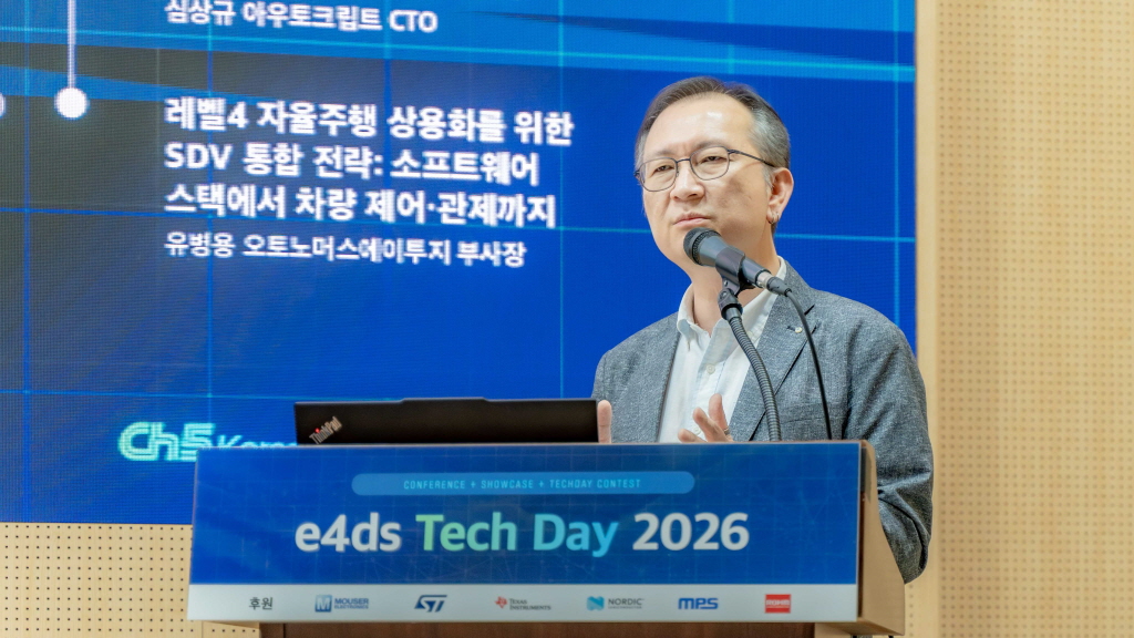
[e4ds Tech Day 2026 ⑨] Sim Sang-gyu, Autocrypt CTO: "In the Physical AI Era, Automotive Security Must Extend Beyond the Vehicle"
At e4ds Tech Day 2026, Sim Sang-gyu, CTO of Autocrypt, explained automotive cybersecurity strategies in the era of Physical AI and SDV (Software-Defined Vehicle). Automobiles are evolving as part of an ecosystem connected to AI, cloud, chargers, IoT, and robots, and he emphasized that the scope of security must expand beyond the vehicle interior to the entire connected environment. In particular, AI model tampering, adversarial attacks, OTA updates, and EV charger hacking were identified as major threats. He explained that response measures require zero trust, AI model integrity protection, intrusion detection, Security by Design and Default, and full lifecycle security management, and that proactive security system establishment beyond regulatory compliance is critical for securing future mobility competitiveness.
2026.10.12by 배종인 기자
NVIDIA to Invest $1 Billion in U.S. Science Over Next Five Years
NVIDIA has announced plans to invest $1 billion over the next five years to strengthen U.S. scientific and technological competitiveness. The company will enhance cutting-edge artificial intelligence research and development capabilities in key areas including quantum computing, healthcare, and energy security, while expanding support for higher education research institutions and cloud service providers. NVIDIA is participating as a major industry partner in the White House Office of Science and Technology Policy's Genesis Mission, and is promoting supercomputer construction in collaboration with national laboratories including Argonne and Los Alamos.
2026.10.12by 배종인 기자











