



KLA Unveils Two Systems for High-Speed Measurement of Wafer Defects
 Published2020.12.15 10:39
SurfScan SP7XP Wafer Defect Inspection System Announced
KLA today announced the PWG5™ wafer geometry metrology system and the Surfscan® SP7XP wafer defect inspection system, designed to solve leading-edge memory and logic integrated circuit manufacturing challenges.
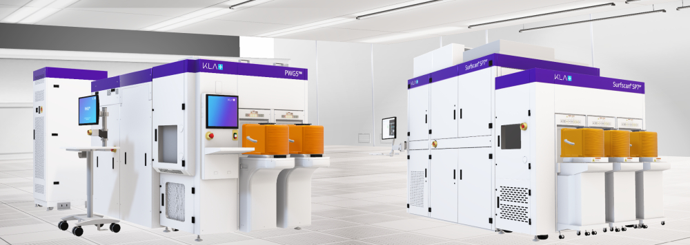
SurfScan SP7XP wafer defect inspection system [Photo = KLA]
Recent flash memory is made with a 3D NAND architecture that stacks layers. Currently, products with 128 layers in a single stack and 176 layers in a double stack are available.
Manufacturing a 3D NAND architecture requires depositing hundreds of thin films of various materials, etching and filling holes that are several microns deep and one-hundredth of a micron wide to create memory cells.
However, as the film stacking increases, stress is induced in the wafer, which changes the wafer surface flatness. Warped wafers affect the uniformity and patterning integrity of subsequent processes, which also adversely affects the performance and yield of the final device.
The PWG5 metrology system measures minute variations in wafer geometry with high resolution to identify and correct patterned wafer variations. This is also possible over a large variation range of inline speeds.
“The complex multilayer nature of 3D NAND architectures places a high demand on wafer geometry measurement,” said Jijen Vazhaeparambil, general manager, Surfscan and ADE business unit at KLA. “The PWG5 has the sensitivity to simultaneously measure flatness variations on the front and back of the wafer.”
“With its inline speed and high resolution support, the PWG5 can be applied not only to 3D NAND but also to DRAM and logic processes,” he said. “Integrated with KLA’s ‘5D Analyzer® data analysis system,’ it supports wafer rework, process equipment recalibration, and lithography system alarms.”
◇ SurfScan SP7XP, Micro-Node Inspection with Machine Learning
With the 3nm (nanometer) node under development, volume production of 5nm node devices is ramping up. EUV lithography is becoming ubiquitous for the most critical layers within these nodes, and device manufacturing is being complicated by new geometries such as finFET or GAA transistor configurations.
Patterning small, complex features billions of times on a wafer in a reproducible manner requires sophisticated defect control, including the use of unpatterned wafer inspectors for careful qualification of starting substrates and materials, and frequent monitoring of processes and equipment.
The SurfScan SP7XP unpatterned wafer defect inspection system offers improved sensitivity and throughput over the SurfScan SP7. Additionally, by introducing machine learning-based defect classification functions, it is possible to detect and identify various defects in a wider range of thin films and substrates.
The equipment is currently used by silicon wafer manufacturers, semiconductor equipment manufacturers developing zero-defect processes, and semiconductor fabs to ensure incoming wafer, process, and equipment quality.
Meanwhile, the PWG5 wafer geometry metrology system and the SurfScan SP7XP wafer defect inspection system are supported by KLA’s global comprehensive service network.
Comments
Related news
KLA Announces eSL10 Electron-Beam Patterned Wafer Defect Inspection System
KLA announced eSL10, an electron beam pattern wafer defect inspection system. The eSL10 is designed to detect and report defects that cannot be detected by conventional optical equipment or other electron beam defect inspection platforms, thereby accelerating the time-to-market for high-performance logic and memory semiconductor chips, including semiconductor chips manufactured through EUV lithography processes.
2020.07.22by 이수민 기자
ACM Research Enters 3D TSV Copper Plating Market
ACM Research announced the Ultra ECP 3D platform for 3D silicon through-silicon via (TSV) technology. The Ultra ECP 3D platform delivers copper electroplating performance without leaving defects such as voids or seams, and is utilized in memory, imaging, MEMS, and optoelectronics applications.
2020.12.04by 이수민 기자
AI semiconductor development, minimizing data movement intervals and memory-centric operations are key
An era has arrived in which how quickly a company processes AI computation is linked to its competitiveness, and demand for semiconductors optimized for AI processing is increasing. For AI semiconductors, parallel processing methods are more suitable than serial processing, and memory-centric design is more appropriate than processor-centric design. For AI semiconductor companies to grow, securing world-class technological capabilities is essential, and communication with downstream industries that use AI semiconductors is equally important.
2020.12.14by 이수민 기자

Intel Unveils Next-Generation 'Core Ultra Series 3' and vPro Platform for Enterprise PCs
Intel has officially unveiled the "Intel Core Ultra Series 3" for next-generation enterprise PCs and the latest vPro platform, addressing a wide range of demands from enterprise notebooks to high-performance workstations.
2026.03.26by 배종인 기자

ROHM Launches ESD Protection Diode Compatible with High-Speed Interfaces of 10Gbps or Higher
Semiconductor specialist ROHM has developed the 'RESDxVx series' of ESD (electrostatic discharge) protection diodes capable of responding to next-generation high-speed data communication environments exceeding 10Gbps, simultaneously enhancing both signal quality maintenance required in high-speed interfaces and IC protection performance.
2026.03.26by 배종인 기자











