


Applied Materials launches new semiconductor inspection equipment based on big data and AI
 Published2021.04.21 08:29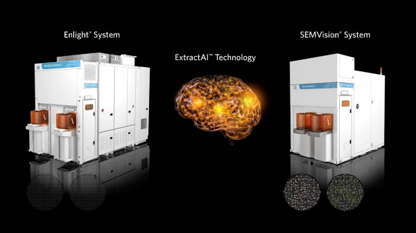
Shortening customer semiconductor chip development time and achieving rapid mass production system
Applied Materials, a global leader in materials engineering solutions, has unveiled an innovative process control system that leverages big data and AI technologies to help semiconductor manufacturers shorten the time it takes to develop and produce semiconductor chips, thereby generating more revenue.
Applied Materials introduced three new semiconductor inspection equipment products at a press conference on the 20th.
The equipment introduced this time are: △The new Enlight optical wafer inspection system, △The new ExtractAI technology, and △The SEMVision electron beam review system.
Five years in development, the new Enlight optical wafer inspection system combines industry-leading high-resolution and high-speed inspection technology, with advanced optical technology that captures more data per scan. The Enlight system architecture delivers economical and efficient optical inspection, reducing the cost of capturing critical defects by three times compared to competitors.
Semiconductor manufacturers can improve the cost aspect through the Enlight system, which allows them to include more inspection steps in the process, and improve 'line monitoring', a statistical process method, by predicting yield-reducing factors more quickly with big data obtained from the system. In addition, by immediately detecting yield-reducing factors, it stops the process when a problem occurs to protect the yield, and by tracing the root cause, it shortens the process improvement time and helps to quickly return to the mass production system.
Applied’s new ExtractAI technology, developed by data scientists at Applied, solves one of the most difficult challenges in wafer inspection by quickly and accurately distinguishing yield-lowering defects from the millions of weak signals and “noise” generated by the latest optical scanners. ExtractAI is the industry’s only solution that connects in real time the big data generated by optical inspection systems with the electron-beam (eBeam) review system that classifies specific yield signals. It infers this big data and classifies all signals on the wafer map, distinguishing yield-lowering factors from noise.
ExtractAI technology is a highly efficient technology that can extract most of the critical defects from a wafer with only a 0.001% level review of potential defects transmitted from the Enlight inspection equipment. This allows semiconductor manufacturers to accelerate semiconductor chip development, production, and yield increase. This AI technology is highly adaptive to wafer conditions, and can quickly identify defects that occur during mass production, while its performance and efficiency gradually improve as more wafers are scanned.
The SEM Vision electron beam review system is the world's most advanced and widely used electron beam review technology. The SEM Vision review system, which provides the industry's highest resolution, and ExtractAI technology classify defects from noise in the wafer detected by the Enlight system, and effectively detect yield-reducing defects. The Enlight system, ExtractAI technology, and SEM Vision system are linked in real time to help customers immediately identify new defects during the manufacturing process, thereby improving yield and profitability. It is compatible with the SEM Vision G7 system, which is widely used in current semiconductor processes, as well as the new Enlight system and ExtractAI technology.
“Quickly and accurately distinguishing yield-lowering defects from noise is a problem semiconductor fabrication engineers have struggled with for more than 30 years,” said Dan Hutcheson, president and CEO of VSLI Research. “Applied Materials’ Enlight System with ExtractAI technology represents a revolutionary way to solve this problem. As the number of systems in use grows, the AI becomes smarter, enabling semiconductor manufacturers to increase their revenue per wafer.”
“Applied’s new playbook for process control combines big data and AI to deliver smart, adaptive solutions that help customers achieve maximum yield in less time,” said Keith Wells, vice president and general manager of Applied Materials’ Imaging Process Control product line.
He added, “By combining industry-leading optical inspection and e-beam review technologies, Applied has created the industry’s only solution that not only detects and classifies yield-critical defects, but also has the intelligence to learn and adapt to process changes in real time. This unique capability enables semiconductor manufacturers to ramp new process nodes faster and reliably detect yield-critical defects throughout the process.”

Comments
Related news

Intel Unveils Next-Generation 'Core Ultra Series 3' and vPro Platform for Enterprise PCs
Intel has officially unveiled the "Intel Core Ultra Series 3" for next-generation enterprise PCs and the latest vPro platform, addressing a wide range of demands from enterprise notebooks to high-performance workstations.
2026.03.26by 배종인 기자

ROHM Launches ESD Protection Diode Compatible with High-Speed Interfaces of 10Gbps or Higher
Semiconductor specialist ROHM has developed the 'RESDxVx series' of ESD (electrostatic discharge) protection diodes capable of responding to next-generation high-speed data communication environments exceeding 10Gbps, simultaneously enhancing both signal quality maintenance required in high-speed interfaces and IC protection performance.
2026.03.26by 배종인 기자

ST Launches 75V Drive IC Targeting 48V Industrial Motor Driving
ST Microelectronics has unveiled the 'STSPIN9P' series of 75V motor drive ICs tailored for 48V-class industrial drive system design. The new product family is characterized by half-bridge and full-bridge configurations that enable design scalability according to motor type and output conditions. Power supply circuits, protection functions, and current sensing circuits are integrated on-chip to simplify system configuration, and the devices are designed to support applications up to 500W maximum. The company plans to provide reference designs and demo boards to support development and evaluation in industrial automation, robotics, pumps, fans, lighting, and textile machinery.
2026.03.26by 배종인 기자

Nordic supports security updates for the entire lifecycle of IoT devices at a single fixed cost
Nordic Semiconductor, a global leader in low-power wireless connectivity solutions, has unveiled a single fixed-cost licensing model that delivers FOTA (Firmware Over-the-Air) and device management capabilities throughout the device lifecycle via nRF Cloud, and introduced a new firmware update solution to prepare for the enforcement of the European Union's Cyber Resilience Act (CRA).
2026.03.26by 배종인 기자

Practical Training in Low-Noise, Low-Power Circuit Design All in One Place… Training Fee Support
The "2026 Advanced Engineer Practical Masterclass" to strengthen competencies in high-sensitivity analog circuit and sensor-based system design will be held on April 16 at the e4ds Conference Center in Gasan-dong, Seoul. This program will be conducted as an offline paid hands-on training session, not online, and is targeted at engineers seeking on-site intensive learning. Texas Instruments will provide educational support for this training, allowing participation at 150,000 won, a 100,000 won discount from the original price of 250,000 won.
2026.03.26by 배종인 기자











