



Materials Science Institute Minimizes Contamination During Semiconductor Linewidth Miniaturization
 Published2021.06.03 09:00
Domestic researchers have succeeded in developing, for the first time in the country, a manufacturing technology for plasma-resistant nanostructured composite ceramics that can resolve the particle issue, which is an obstacle to semiconductor linewidth miniaturization.
A research team led by Dr. Park Young-jo of the Engineering Ceramics Laboratory at the Korea Institute of Materials Science (KIMS, President Lee Jeong-hwan), a government-funded research institute under the Ministry of Science and ICT, announced on the 3rd that they have developed a new plasma-resistant ceramic material, expected to reduce contaminant particles inside semiconductor manufacturing equipment, for the first time in Korea through joint research with Mico Ceramics Co., Ltd. (CEO Yeo Moon-won).
In semiconductor manufacturing, a plasma-based etching process is generally performed. At this time, not only the silicon wafer but also the internal components of the equipment are exposed to plasma irradiation, generating contaminant particles that become a major cause of chip defects.
As semiconductor linewidths become finer, high-power plasma etching is required, leading to an urgent need for the development of new plasma-resistant materials to minimize the generation of contaminant particles.
When irradiating with plasma for material etching, the two variables for preventing contaminant particles are maintaining a 'low etching rate' and 'low surface roughness'.
The research team applied the pore-free theoretical density densification sintering technology, previously used in the development of transparent ceramics, to yttria-magnesia (Y2O3·MgO) composite ceramics to achieve a fully dense sintered body without residual pores, thereby minimizing the etching rate.
In addition, by combining yttria (Y2O3) and magnesia (MgO), which have verified plasma resistance, and minimizing grain growth during the sintering process, it was confirmed that the lowest surface roughness was achieved by achieving a microstructure at the 300 nanometer (nm) level.
The semiconductor industry is a key national industry in which Korea has secured the status of a first mover.
On the other hand, a significant portion of the advanced process equipment in manufacturing lines still relies heavily on overseas sources. The results of this study are highly significant in that they developed a world-class plasma-resistant material using domestic technology, advanced process equipment utilizing this material, and secured a technological advantage in the global competition for linewidth miniaturization.
"Senior Researcher Kim Ha-neul of the research team stated, 'This research result is highly significant as it is the first to prove that even with different materials, manufacturing dense materials and components with uniform, small-sized crystal grains can actually improve the reliability of semiconductor process equipment compared to materials and components made of a single material, and that this finding has been internationally recognized.'"
This research was conducted with support from the Ministry of Science and ICT's 'Nano and Materials Technology Development Project (National Core Materials Research Group).' Additionally, the research results were published in the world-renowned academic journal Scientific Reports on May 13. Meanwhile, a PCT patent application for the related technology has been completed.
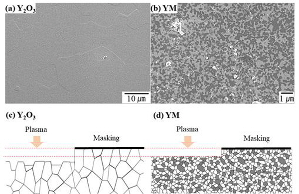
▲ Electron microscope microstructure (a,b) and etching schematic (c,d) of single-phase Y2O3 and composite material Y2O3·MgO

Comments
Related news
Korea Institute of Materials Science Takes the Lead in Realizing Carbon Neutrality
The Korea Institute of Materials Science (KIMS, Director Lee Jung-hwan), a government-funded research institute under the Ministry of Science and ICT, has established the 'Carbon-Neutral Materials Technology Research Planning Group' and will actively engage in research in the materials technology sector for realizing carbon neutrality, as well as planning and discovering related projects.
2021.05.06by 배종인 기자

Materials Research Institute Develops Corona Antiviral Verification Mask
The Korea Institute of Materials Science (KIMS, Director Lee Jeong-hwan) has completed the development of a mask with verified anti-viral performance against COVID-19, raising expectations that it will contribute to preventing COVID-19 infection.
2021.05.11by 배종인 기자
KIMS, Dr. Han Seung-jeon's Team '2020 Outstanding Achievements by Government-funded Research Institutes'
The research team led by Dr. Han Seung-jeon of the Special Alloys Research Division at the Metal Materials Research Division of the Korea Institute of Materials Science (KIMS, Director Lee Jeong-hwan), a government-funded research institute under the Ministry of Science and ICT, was selected for the '2020 Outstanding Research Results of Government-Funded Research Institutes' and received the Minister's Award from the Ministry of Science and ICT.
2021.05.20by 배종인 기자

Intel Unveils Next-Generation 'Core Ultra Series 3' and vPro Platform for Enterprise PCs
Intel has officially unveiled the "Intel Core Ultra Series 3" for next-generation enterprise PCs and the latest vPro platform, addressing a wide range of demands from enterprise notebooks to high-performance workstations.
2026.03.26by 배종인 기자

ROHM Launches ESD Protection Diode Compatible with High-Speed Interfaces of 10Gbps or Higher
Semiconductor specialist ROHM has developed the 'RESDxVx series' of ESD (electrostatic discharge) protection diodes capable of responding to next-generation high-speed data communication environments exceeding 10Gbps, simultaneously enhancing both signal quality maintenance required in high-speed interfaces and IC protection performance.
2026.03.26by 배종인 기자











