



Materials Research Institute Uses AI to Identify Ultra-Fine Defects
 Published2021.07.19 16:07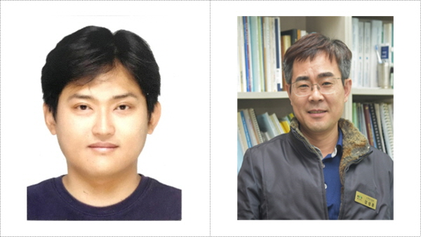
▲The principal investigators of this study, Dr. Moon In-yong (left) and Dr. Kang Seong-hun (right) of the Korea Institute of Materials Science
A domestic research team has succeeded in developing a technology that can automatically recognize ultra-fine defects on surfaces with complex shapes.
The research team led by Dr. Kang Sung-hoon of the Materials Artificial Intelligence and Big Data Laboratory at the Korea Institute of Materials Science (KIMS, President Lee Jeong-hwan), a government-funded research institute under the Ministry of Science and ICT, has developed a technology that can accurately detect ultra-fine defects on the surface of products that are difficult for humans to distinguish using artificial intelligence (AI) technology.
Minor defects in products appear in various forms, and visually checking and inspecting them results in a lot of time and cost loss. In particular, the surface of parts with complex hierarchical structures has a three-dimensional shape, making it somewhat difficult to obtain accuracy using only a microscope or visual inspection.
To solve these problems, the research team succeeded in developing artificial intelligence (AI) technology that automatically recognizes the hierarchical structure of a product's surface through an image that simplifies a three-dimensional shape into a two-dimensional shape and detects micro-defects that deviate from the reference image.
The applied artificial neural network automatically learns the characteristics of defective factors and then performs defect detection and classification.
In particular, ultra-fine defects, which are half the thickness of a human hair (50㎛), are impossible to accurately read with the naked eye, so workers had to take dozens of photos of each specimen using a microscope and check them one by one. However, using this technology, it is possible to accurately detect defective factors in just one second or so.
In addition to defect detection, the Class Activation Map (CAM) neural network was applied to allow users to know which surface features the artificial intelligence (AI) used to select defects, thereby increasing the reliability of ultra-fine defect detection.
“Process automation and smart factory construction have recently become social issues,” said Kang Seong-hun, the research director and principal researcher. “If the developed technology is applied to various automated process lines, it is expected that even minute defects that are difficult for humans to read will be detectable in a short period of time.”
This research was conducted with support from the Ministry of Trade, Industry and Energy's 'Virtual Engineering Platform Construction Project for Lightweight Materials for Automotive' and the Korea Institute of Materials Science's major projects.
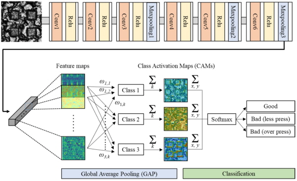
▲An artificial intelligence neural network structure used to detect defects on hierarchical pattern surfaces.

Comments
Related news

Materials Science Institute, Contest for Popularization of Materials, Parts, and Equipment… Grand Prize 1 Million Won
The Korea Institute of Materials Science (KIMS, Director Lee Jeong-hwan) is hosting a "Democratization of Materials, Parts and Equipment Contest." The Grand Prize winner (or team) will receive a certificate and 1 million won in prize money; two Excellence Award winners (or teams) will each receive a certificate and 500,000 won; and five Encouragement Award winners (or teams) will each receive a certificate and 200,000 won.
2021.06.21by 배종인 기자
Materials Research Institute and Gyeongnam Provincial Police Agency Integrating Science and Technology into Security Fields
The Korea Institute of Materials Science (KIMS, Director Lee Jeong-hwan), a government-funded research institute under the Ministry of Science and ICT, and the Gyeongnam Provincial Police Agency (Commissioner Lee Mun-su) have joined hands to enhance investigative capabilities by integrating science and technology into law enforcement operations.
2021.06.30by 배종인 기자
Materials Research Institute Expands Investment in Future Mobility Technology
The Korea Institute of Materials Science (KIMS, Director Lee Jung-hwan), a government-funded research institute under the Ministry of Science and ICT, has announced the recruitment and selection of demand companies in the 'future mobility new industry sector' and committed to investment support for resolving core technical challenges and commercialization.
2021.07.07by 배종인 기자
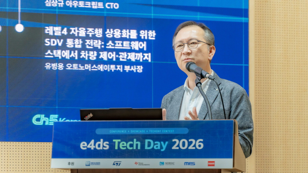
[e4ds Tech Day 2026 ⑨] Sim Sang-gyu, Autocrypt CTO: "In the Physical AI Era, Automotive Security Must Extend Beyond the Vehicle"
At e4ds Tech Day 2026, Sim Sang-gyu, CTO of Autocrypt, explained automotive cybersecurity strategies in the era of Physical AI and SDV (Software-Defined Vehicle). Automobiles are evolving as part of an ecosystem connected to AI, cloud, chargers, IoT, and robots, and he emphasized that the scope of security must expand beyond the vehicle interior to the entire connected environment. In particular, AI model tampering, adversarial attacks, OTA updates, and EV charger hacking were identified as major threats. He explained that response measures require zero trust, AI model integrity protection, intrusion detection, Security by Design and Default, and full lifecycle security management, and that proactive security system establishment beyond regulatory compliance is critical for securing future mobility competitiveness.
2026.10.12by 배종인 기자

NVIDIA to Invest $1 Billion in U.S. Science Over Next Five Years
NVIDIA has announced plans to invest $1 billion over the next five years to strengthen U.S. scientific and technological competitiveness. The company will enhance cutting-edge artificial intelligence research and development capabilities in key areas including quantum computing, healthcare, and energy security, while expanding support for higher education research institutions and cloud service providers. NVIDIA is participating as a major industry partner in the White House Office of Science and Technology Policy's Genesis Mission, and is promoting supercomputer construction in collaboration with national laboratories including Argonne and Los Alamos.
2026.10.12by 배종인 기자











