



Cadence Launches Machine Learning-Based EDA, Improving PPA
 Published2021.08.02 11:10
Productivity up to the system semiconductor sign-off stage
Supports up to 10x and 20% PPA improvement
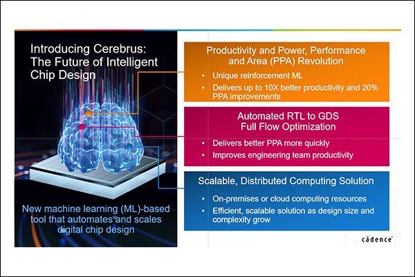
On the 2nd, Cadence launched the machine learning-based 'Cerebrus™ Intelligent Chip Explorer' tool that supports digital chip design automation and achieving chip design goals. Engineers can quickly identify flow solutions that are difficult to design explore, improving productivity and reducing power consumption by 20% to improve Power Performance Area (PPA).
Cerebus works with Cadence's synthesis solution (Genus™), automated place and route implementation system (Innovus™), timing signoff solution (Tempus™), RTL power solution (Joules™), IC power integrity solution (Voltus™), and physical verification signoff solution (Pegasus™) to provide customers with a path to improved verification and predictability.
The combination of the new product and the Cadence RTL-to-signoff flow will increase the productivity of chip designers, CAD and IP developers by up to 10x compared to traditional manual methods, and help improve power and PPA by up to 20%.
With enhanced machine learning capabilities, Cerebus quickly identifies flow solutions that engineers might not explore, and automatically applies design learnings to future designs, reducing the iteration time required to achieve better results.
Additionally, Cadence Cerebus enables a single engineer to optimize and parallelize the entire RTL-to-GDS flow across multiple design blocks simultaneously, increasing productivity across the entire design team. Additionally, it accelerates flow optimization with a scalable design exploration method that can be used on-premises or in the cloud.
“As we provide the latest semiconductor processes, we place the utmost importance on the efficiency of our Design Technology Co-Optimization (DTCO) program,” said Kim Sang-yoon, senior vice president of Samsung Foundry Design Technology. “We are continuously exploring ways to improve PPA and productivity in chip implementation.”
He continued, "Samsung Foundry has used Cerebus and Cadence digital implementation flows across multiple application products, reducing work that previously took months to complete in just days, and has seen power savings of more than 8% in some of the most critical design blocks." He added that the final design development time has been improved by more than 50%.
“Cerebrus and Cadence Systems’ semiconductor signoff tools will enable a new approach to the development of advanced design projects by increasing design performance by more than 10% through automated flow optimization and floorplan exploration,” said Satoshi Shibatani, Digital Design Director, EDA Division, Renesas Shared R&D.
“As the industry continues to move to more advanced processes, design complexity is increasing,” said Chin-Chi Teng, Senior Vice President and General Manager of Cadence Digital & Signoff Group. “Cerebrus is the solution that efficiently achieves PPA goals.”
Comments
Related news
.jpg)
Xilinx Announces Vivado FPGA EDA Tool, Powered by Machine Learning
Today's EDA designers are facing challenges with increasing design complexity. In response, Xilinx has launched "Vivado ML Edition," an FPGA EDA tool that reduces design time and cost based on machine learning (ML) optimization algorithms and team-based design flow. Compared to the existing "Vivado HLx Edition," it guarantees 5x faster compilation time on complex designs and average result quality improvements of 10%.
2021.06.25by 이수민 기자
The Ministry of Trade, Industry and Energy announced that the power semiconductor commercialization project achieved 39 billion won in results.
The Ministry of Trade, Industry and Energy conducted a review on the 21st of the commercialization project outcomes for power semiconductors aimed at creating new industries. The project has been carried out from 2017 through 2023 to establish a domestic industrial foundation for power semiconductors based on compound materials such as Si, SiC, and GaN. During this review, it was confirmed that commercialization results worth approximately 39 billion won were generated from 2019 through May of this year through product development by participating companies.
2021.07.21by 이수민 기자

The Korea Semiconductor Association (KSA) welcomes the tax law revisions, which will support semiconductors, batteries, and vaccines.
The Korea Semiconductor Industry Association, Korea Bio Association, and Korea Battery Industry Association have expressed their support for tax law amendments that provide support for three major emerging industries including semiconductors, batteries, and vaccines.
2021.07.28by 배종인 기자

Intel Unveils Next-Generation 'Core Ultra Series 3' and vPro Platform for Enterprise PCs
Intel has officially unveiled the "Intel Core Ultra Series 3" for next-generation enterprise PCs and the latest vPro platform, addressing a wide range of demands from enterprise notebooks to high-performance workstations.
2026.03.26by 배종인 기자

ROHM Launches ESD Protection Diode Compatible with High-Speed Interfaces of 10Gbps or Higher
Semiconductor specialist ROHM has developed the 'RESDxVx series' of ESD (electrostatic discharge) protection diodes capable of responding to next-generation high-speed data communication environments exceeding 10Gbps, simultaneously enhancing both signal quality maintenance required in high-speed interfaces and IC protection performance.
2026.03.26by 배종인 기자











