


KIMM Successfully Localizes 400nm-Class Lithography Equipment
 Published2021.08.13 13:56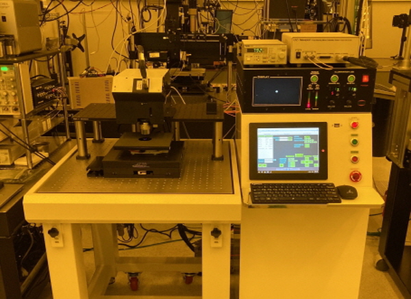
400nm-class laser direct lithography equipment developed by the research team of Research Fellow Lee Jae-jong and Principal Researcher Lim Hyung-jun of the Nano Process Equipment Research Laboratory at the Korea Institute of Mechanical Engineering
The Korea Institute of Machinery and Materials (KIMM, President Park Sang-jin), under the Ministry of Science and ICT, has succeeded in localizing 400 nm (nanometer) class laser direct lithography equipment for the first time in Korea. It is attracting attention as a technology that can dramatically improve semiconductor productivity.
The Korea Institute of Machinery and Materials announced on the 12th that a research team led by Research Fellow Lee Jae-jong and Principal Researcher Lim Hyung-jun of the Nano Process Equipment Research Laboratory has developed a laser lithography machine capable of processing resist coated on a substrate by moving a fine focus at the 400 nm level at a speed of 40 mm per second.
Laser lithography is a technology that can create very small shapes by focusing a laser beam on a resist on a substrate, causing the resist to react to the light and harden.
The research team succeeded in creating a very fine focus of 400 nm using a blue-violet laser diode with a wavelength of 405 nm among various lasers and processing a substrate using it.
Using the equipment developed by the research team, the laser focus moves over a 200 mm substrate at a speed of 40 mm per second, allowing for processing as if drawing on a canvas with a fine pen.
In addition, to shorten the process time that increases as it is applied to a large area with a small focus, we devised a technology that can increase the process line width by up to 50 times and filed a patent.
Nano-level lithography technology is gaining attention as one of the next-generation semiconductor lithography technologies. Currently, commercialized lithography technology is being led by countries such as Germany and the Netherlands. This is the first time in Korea that precise patterns at the 400 nm level have been implemented on planar and non-planar substrates.
By applying the technology developed this time, it is possible to realize three-dimensional nano-micro composite structures that are difficult to realize with existing lithography technology, as well as to realize nanostructures on surfaces of arbitrary shapes.
This is expected to be utilized in the future for the fabrication of biosensors, medical devices, micro-optical devices, and microfluidic channels. In addition, it is expected to have the effect of replacing expensive foreign equipment.
Based on their research capabilities, including the successful development and commercialization of large-area nanoimprint process equipment through a national R&D project, Dr. Lee Jae-jong's research team was able to enhance the commercialization potential of research equipment by developing a new concept of laser lithography equipment and advancing the technology.
“Direct laser lithography is a representative technology where various fields such as mechanics, optics, materials, and electronics converge,” said Principal Researcher Im Hyeong-jun. “It can dramatically improve the economic efficiency of production processes, so it is expected to secure leadership in the global market in the future.”
Meanwhile, this research was conducted with support from the 'Development of 3D Nano-Micro Hybrid Structure Fabrication Platform and IVD (In-Verbal Diagnosis) System Integration Technology' project, funded by the H-Guard Research Group (Ministry of Science and ICT Global Frontier Project), and the 'Development of Freeform Nanofabrication Processes and Systems and Applications to Non-Hematological Disease Monitoring Devices' project under the Nanomaterials Technology Development Program.

Comments
Related news
Korea Institute of Machinery and Materials (KIMM) excels in AI safety diagnosis
The Korea Institute of Machinery and Materials is demonstrating excellent performance in monitoring the condition of equipment and structures across various sectors including defense, public, and industrial fields, and proactively diagnosing and preventing failures through the commercialization of IoT (Internet of Things), big data, and AI-based predictive maintenance technology.
2021.07.19by 배종인 기자
Korea Mechanical Engineering & Construction Co., Ltd. develops optimal welding technology for high manganese steel
The Korea Institute of Machinery and Materials (KIMM), under the Ministry of Science and ICT, with director Park Sang-jin, has developed optimal hybrid laser-arc welding for manufacturing LNG high-manganese fuel tanks, raising expectations that it will further enhance the competitiveness of Korea's shipbuilding industry.
2021.07.22by 배종인 기자
.jpg)
Korea Institute of Machinery and Materials (KIMM) looks at hydrogen machine technology
The Korea Institute of Machinery and Materials will hold the "2021 Global Forum on Mechanical Engineering" online on September 8th with the theme of "Hydrogen Mechanical Engineering as the Foundation for Carbon Neutrality."
2021.08.09by 배종인 기자

Intel Unveils Next-Generation 'Core Ultra Series 3' and vPro Platform for Enterprise PCs
Intel has officially unveiled the "Intel Core Ultra Series 3" for next-generation enterprise PCs and the latest vPro platform, addressing a wide range of demands from enterprise notebooks to high-performance workstations.
2026.03.26by 배종인 기자

ROHM Launches ESD Protection Diode Compatible with High-Speed Interfaces of 10Gbps or Higher
Semiconductor specialist ROHM has developed the 'RESDxVx series' of ESD (electrostatic discharge) protection diodes capable of responding to next-generation high-speed data communication environments exceeding 10Gbps, simultaneously enhancing both signal quality maintenance required in high-speed interfaces and IC protection performance.
2026.03.26by 배종인 기자











