


ACM Secures Order for Wafer Equipment for Compound Semiconductors
 Published2021.09.14 16:41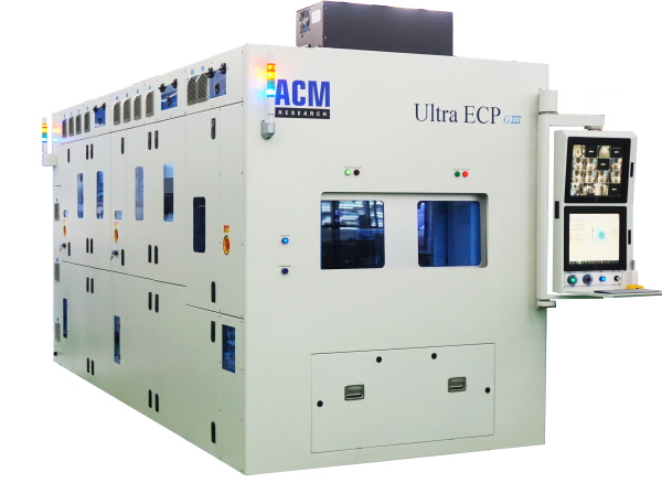
Optimized edge and notch pattern, achieving plating uniformity of less than 3%
ACM Research, Inc. announced the launch of wafer-level packaging and plating support equipment for compound semiconductor manufacturing and secured multiple orders for related equipment in the third quarter.
ACM Research announced on the 14th that it has recently launched the Ultra ECP GIII electroplating equipment, a wafer-level packaging product for compound semiconductors capable of supporting silicon carbide (SiC), gallium nitride (GaN), and gallium arsenide (GaAs).
Additionally, ACM's Ultra ECP GIII has reportedly received two orders from Chinese compound semiconductor manufacturers.
The first order equipment was delivered to the customer after applying a plating module composed of copper-nickel-tin-silver using secondary anode technology to wafer-level packaging and integrating it into a vacuum pre-wet chamber and a post-clean chamber. The second order equipment is for gold (Au) plating and is scheduled to be finally supplied to the customer at the end of September.
This wafer-level packaging equipment can plate gold (Au) with improved uniformity and step coverage in the backside deep hole process.
It also features a fully automated platform that supports high-volume processing of 6-inch flat edge and notch wafers, and achieves the highest performance by combining ACM's proprietary second anode supply technology with high-speed paddle technology.
“The compound semiconductor market is growing rapidly due to strong demand for electric vehicles, 5G communications, RF and AI applications. However, the automation level of current compound semiconductor manufacturing processes is limited, and most electroplating processes use vertical electroplating equipment with poor uniformity, which also limits production volume,” said David Wang, CEO of ACM Research. “Our newly developed Ultra ECP GIII electroplating equipment overcomes these challenges and meets the growing requirements for high capacity and advanced performance of compound semiconductors.”
ACM's Ultra ECP GIII tool leverages two key technologies: a secondary anode supply and high-speed grid technology. The secondary anode supply provides superior uniformity control by effectively adjusting wafer-level packaging features to overcome issues arising from differences in electrical field distribution. Additionally, this technology can be utilized to optimize patterns in wafer edge and notch areas and achieve plating uniformity of less than 3%.
ACM's high-speed grid technology achieves a more powerful mixing effect and enhances mass transfer capabilities, improving step coverage in deep-hole processes. Furthermore, improved step coverage reduces gold (Au) film thickness, thereby reducing customer costs.

Comments
Related news
ACM Research Enters 3D TSV Copper Plating Market
ACM Research announced the Ultra ECP 3D platform for 3D silicon through-silicon via (TSV) technology. The Ultra ECP 3D platform delivers copper electroplating performance without leaving defects such as voids or seams, and is utilized in memory, imaging, MEMS, and optoelectronics applications.
2020.12.04by 이수민 기자
ACM Unveils New Equipment for Logic and Power Semiconductor Furnace Processes
In the latest semiconductor processes, requirements for temperature control uniformity and stability in thermal processing are increasingly stringent to maintain wafer yield. In response, ACM Research has added undoped and doped poly deposition, gate oxide deposition, high-temperature oxidation, and annealing process equipment to its 300mm dry process system.
2021.04.07by 이수민 기자
ACM Research to Supply Wafer Wet Etcher ‘Bevel Etch’
During IC manufacturing processes in 3D NAND, DRAM, and advanced logic nodes, wafer edge yield degradation is occurring due to wafer edge delamination, particles, and residues. To address this issue, the need to improve overall process yield is growing. ACM Research's bevel etch equipment uses wet etch technology to remove various dielectric, metal, and organic material films from wafer edges as well as particulate contaminants.
2021.08.26by 이수민 기자

Intel Unveils Next-Generation 'Core Ultra Series 3' and vPro Platform for Enterprise PCs
Intel has officially unveiled the "Intel Core Ultra Series 3" for next-generation enterprise PCs and the latest vPro platform, addressing a wide range of demands from enterprise notebooks to high-performance workstations.
2026.03.26by 배종인 기자

ROHM Launches ESD Protection Diode Compatible with High-Speed Interfaces of 10Gbps or Higher
Semiconductor specialist ROHM has developed the 'RESDxVx series' of ESD (electrostatic discharge) protection diodes capable of responding to next-generation high-speed data communication environments exceeding 10Gbps, simultaneously enhancing both signal quality maintenance required in high-speed interfaces and IC protection performance.
2026.03.26by 배종인 기자











