


Samsung Electronics begins mass production of 14nm EUV DDR5 DRAM.
 Published2021.10.12 11:00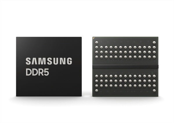
▲Samsung Electronics' industry-leading 14nm DDR5 DRAM
Twice the speed of DDR4, 20% power consumption improvement compared to previous generations
Samsung Electronics has achieved the industry's highest wafer density by mass producing the industry's most advanced 14nm DRAM using the EUV (Extreme Ultra-Violet) process, thereby improving productivity by approximately 20%.
Samsung Electronics announced on the 12th that it has begun mass production of 14nm EUV DDR5 DRAM.
Samsung Electronics was the first in the industry to supply DRAM modules using the EUV process to customers in March 2020, and is showcasing differentiated process technologies such as the industry's only implementation of the EUV multilayer process to create cutting-edge 14nm DRAM.
Samsung Electronics plans to secure a firm edge in the competition for fine DRAM processes below 14nm by applying EUV lithography technology, which can implement semiconductor circuits in greater detail, to improve the performance and yield of DRAM.
Samsung Electronics' 14nm DRAM, which uses the EUV process on five layers, boasts the industry's highest wafer density and boasts productivity that is approximately 20% higher than the previous generation.
Additionally, the power consumption of Samsung Electronics' 14nm DRAM products has been improved by approximately 20% compared to the previous process. />
Samsung Electronics was the first to apply this new process to the latest DDR5 (Double Data Rate 5) DRAM.
DDR5 is a next-generation DRAM standard that is more than twice as fast as DDR4, with a maximum speed of 7.2 Gbps. As data utilization methods such as artificial intelligence and machine learning become more advanced, demand for high-performance DDR5 is continuously increasing in data centers, supercomputers, and enterprise server markets.
Samsung Electronics' strategy is to lead the popularization of DDR5 DRAM by implementing differentiated performance and stable yield based on the industry's most advanced 14nm process and highly mature EUV process technology.
Additionally, Samsung Electronics plans to mass-produce up to 24Gb DRAM, the maximum capacity for a single chip, through this process to actively respond to the demand for high-capacity data in the market.
“Samsung Electronics has overcome the limitations of semiconductor microfabrication processes through continuous technological innovation over the past 30 years, and this time, we have implemented the industry’s most advanced 14nm process by being the first to apply the EUV process to multi-layers,” said Lee Ju-young, Senior Vice President and Head of DRAM Development at Samsung Electronics’ Memory Business. “We will supply the best memory solutions needed in the era of big data, such as 5G, AI, and the metaverse, with high capacity, high performance, and high productivity.”

Comments
Related news
Samsung Electronics Develops 512GB DDR5 Module, "Expected to Launch in Second Half"
The next-generation DRAM specification, DDR5, delivers twice the performance of DDR4. With data transfer speeds reaching approximately 7200Mbps, it can process two 30GB capacity UHD movies in a single second. Samsung Electronics has developed a 512GB DDR5 memory module with the industry's largest capacity by applying HKMG process technology and 8-level TSV technology to DRAM for the first time.
2021.03.29by 이수민 기자
Samsung Electronics Launches New uMCP Products, Incorporating DRAM and NAND in a Single Chip
Samsung Electronics has enhanced design convenience and space utilization for smartphone manufacturers through the launch of a high-performance uMCP new product that integrates DRAM and NAND flash memory on a single chip.
2021.06.15by 배종인 기자
Samsung Electronics Expands AI Memory Market
Samsung Electronics is expanding its lineup of memory semiconductor products equipped with AI engines. Samsung Electronics will lead the convergence and integration of memory and system semiconductors, and plans to rapidly expand the next-generation memory semiconductor ecosystem through collaborations with various global companies.
2021.08.24by 배종인 기자

Intel Unveils Next-Generation 'Core Ultra Series 3' and vPro Platform for Enterprise PCs
Intel has officially unveiled the "Intel Core Ultra Series 3" for next-generation enterprise PCs and the latest vPro platform, addressing a wide range of demands from enterprise notebooks to high-performance workstations.
2026.03.26by 배종인 기자

ROHM Launches ESD Protection Diode Compatible with High-Speed Interfaces of 10Gbps or Higher
Semiconductor specialist ROHM has developed the 'RESDxVx series' of ESD (electrostatic discharge) protection diodes capable of responding to next-generation high-speed data communication environments exceeding 10Gbps, simultaneously enhancing both signal quality maintenance required in high-speed interfaces and IC protection performance.
2026.03.26by 배종인 기자











