


ACM, SAPS demo equipment order secured
 Published2021.11.10 16:49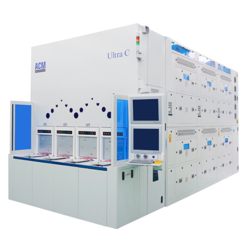
▲ ACM's SAPS Advanced Wafer Cleaning System
ACM Research, Inc., a leader in wafer handling solutions for semiconductor and advanced WLP (Wafer-Level Packaging) applications, is expanding business and collaboration opportunities by securing orders for SAPS demo equipment from major global semiconductor manufacturers.
ACM Research announced on the 10th that it has received an order for a trial version of its Ultra C SAPS full-surface cleaning equipment from a major global semiconductor manufacturer. The equipment is scheduled to be installed at the customer's development fab in China during the first quarter of 2022.
“This order from a global semiconductor company operating a fab in China is a tremendous opportunity for us,” said Dr. David Wang, CEO of ACM Research. “This semiconductor company decided to evaluate ACM’s SAPS technology as part of its efforts to improve its R&D capabilities and production processes.” “By successfully completing this equipment evaluation, we look forward to continuing more business and cooperation opportunities with this client as well as other key customers in the region,” he said.
ACM’s proprietary SAPS™ (Space Alternated Phase Shift) advanced wafer cleaning technology utilizes the phase shift of megasonic waves in the gap between the megasonic transducer and the wafer. Unlike the fixed megasonic transducers used in conventional megasonic wafer cleaning systems, SAPS technology moves or tilts the transducer while the wafer rotates, ensuring that megasonic energy is delivered uniformly to every point on the wafer even when the wafer is warped. SAPS technology offers significantly faster processing speeds than conventional megasonic cleaning methods and does not damage the wafer surface or cause material loss. Furthermore, SAPS technology has demonstrated the ability to achieve more thorough and comprehensive cleaning capabilities without compromising device functionality, even in sub-10 nanometer ultrafine processes.

Comments
Related news
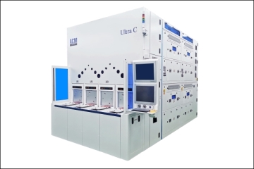
ACM Research to Supply Wafer Wet Etcher ‘Bevel Etch’
During IC manufacturing processes in 3D NAND, DRAM, and advanced logic nodes, wafer edge yield degradation is occurring due to wafer edge delamination, particles, and residues. To address this issue, the need to improve overall process yield is growing. ACM Research's bevel etch equipment uses wet etch technology to remove various dielectric, metal, and organic material films from wafer edges as well as particulate contaminants.
2021.08.26by 이수민 기자
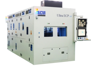
ACM Secures Order for Wafer Equipment for Compound Semiconductors
ACM Research, Inc. has launched wafer-level packaging and plating support equipment for compound semiconductor manufacturing, and is reported to have secured multiple orders for related equipment in the third quarter.
2021.09.14by 배종인 기자
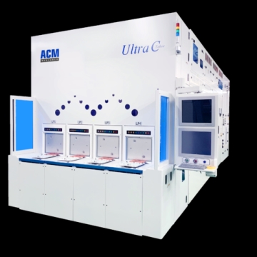
ACM Launches 300mm Single-Wafer SPM Equipment
ACM Research, Inc., a leading provider of wafer processing solutions for semiconductor and advanced WLP (Wafer-Level Packaging) applications, is building a diverse portfolio in the wet cleaning field through new equipment for advanced semiconductor wafer manufacturing, including advanced logic, DRAM, and 3D NAND.
2021.10.05by 배종인 기자

Intel Unveils Next-Generation 'Core Ultra Series 3' and vPro Platform for Enterprise PCs
Intel has officially unveiled the "Intel Core Ultra Series 3" for next-generation enterprise PCs and the latest vPro platform, addressing a wide range of demands from enterprise notebooks to high-performance workstations.
2026.03.26by 배종인 기자

ROHM Launches ESD Protection Diode Compatible with High-Speed Interfaces of 10Gbps or Higher
Semiconductor specialist ROHM has developed the 'RESDxVx series' of ESD (electrostatic discharge) protection diodes capable of responding to next-generation high-speed data communication environments exceeding 10Gbps, simultaneously enhancing both signal quality maintenance required in high-speed interfaces and IC protection performance.
2026.03.26by 배종인 기자











