



Korean and Chinese researchers develop new semiconductor material to replace silicon
 Published2021.11.16 13:48
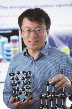 Korean and Chinese research teams have successfully fabricated large-area single crystals of a new material to replace silicon-based semiconductor materials that have reached the limits of technological performance, raising expectations for future mass production.
The research team led by Feng Ding, group leader at the Institute for Basic Science (IBS, Director Noh Do-young) Center for Multidimensional Carbon Materials (Distinguished Professor, Department of Materials Science and Engineering, UNIST), announced on the 16th that it has elucidated key principles affecting large-area single crystal growth of transition metal dichalcogenides in collaboration with researchers from Peking University and other Chinese research institutions.
The joint research team has also succeeded in fabricating representative transition metal dichalcogenide (TMD) materials such as tungsten disulfide (WS2) as wafer-size single crystals.
Transition Metal Dichalcogenides (TMD) with excellent physical and electrical properties have attracted attention as next-generation semiconductor materials alongside graphene and black phosphorus. Research institutes worldwide are competitively studying this material, but mass production has not yet been achieved.
In particular, dichalcogenides have faced difficulties in wafer manufacturing due to the complexity of substrate selection, resulting in non-uniform alignment of small single crystals grown through epitaxial growth and their positioning at edges, making it difficult to produce high-performance wafers.
In this research, the joint research team presented the principle of selecting customized transition metal dichalcogenide substrates with unique symmetric structures based on theoretical calculations, and named this method 'double-bond-induced epitaxial growth'.
For example, in the case of tungsten disulfide (WS2), the synthesis process favors two antiparallel directions. When sapphire, an insulator, is used as the substrate, all tungsten disulfide grown from step edges on the substrate aligns in a single direction. Crystal grains at the step edges gradually grow, ultimately forming a large-area single crystal of the same size as the substrate.
First author Ting Cheng, a researcher, explained that "based on the 'double-bond-induced epitaxial growth method', by selecting an appropriate substrate, it is theoretically possible to grow all 2D materials as large-area single crystals."
In the same manner, the joint research team succeeded in fabricating transition metal dichalcogenides such as molybdenum disulfide (MoS2), tungsten diselenide (WSe2), and molybdenum diselenide (MoSe2) at a 2-inch wafer-size large area. This marks a breakthrough that can dramatically accelerate the practical application of new semiconductor materials to succeed silicon.
Feng Ding, group leader, stated, "Following graphene and hexagonal boron nitride (hBN), the 'senior' materials in the 2D materials field, transition metal dichalcogenides can now be fabricated as wafer-size single crystals. This is a landmark study in the history of 2D materials research that will lead advances in high-performance electronic and optoelectronic device fields."
The research results were published on November 16 in Nature Nanotechnology (IF 39.213), an authoritative journal in the field of nanoscience.
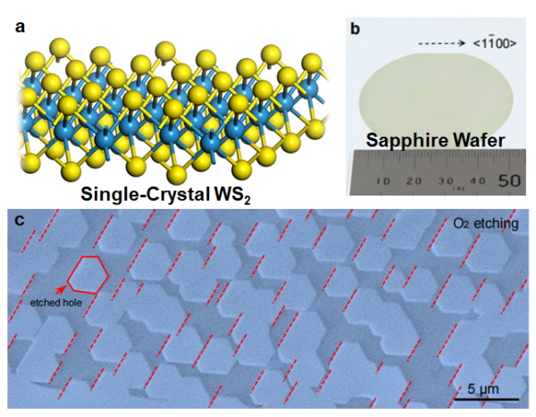
▲Growth of tungsten disulfide on an insulator

Comments
Related news
Wiring spacing within semiconductor devices can be further reduced
A research team led by Professor Shin Hyun-seok at UNIST has successfully developed an ultra-low dielectric constant insulator that enables more precise fabrication of semiconductor devices through collaborative research with Samsung Electronics' Advanced Institute of Technology, IBS, and others. The insulators currently used in semiconductor processes are porous organosilicates with a dielectric constant of approximately 2.5. The amorphous boron nitride synthesized by the research team in this study has a dielectric constant of 1.78, representing the discovery of a novel material with a dielectric constant below 2.5, which has been regarded as a technical challenge.
2020.06.25by 이수민 기자
Black phosphorus, could it become the main material for angstrom semiconductors smaller than nanometers?
The IBS Multidimensional Carbon Materials Research Group has realized a conductive channel with a linewidth of 0.43nm using two-dimensional black phosphorus. Two-dimensional black phosphorus is considered a leading semiconductor device for the post-graphene era. With a thickness of approximately one atomic layer, it can be applied to flexible and transparent devices that are difficult to implement with silicon-based semiconductors. Additionally, it exhibits the highest electron mobility among two-dimensional semiconductor devices.
2021.07.30by 이수민 기자

IBS celebrates its 10th anniversary with a variety of events, including lectures by Nobel laureates.
The Institute for Basic Science (IBS, Director No Do-young) has organized various science concerts, including lectures by Nobel Prize laureates, to commemorate its 10th anniversary since its establishment.
2021.11.08by 배종인 기자

Intel Unveils Next-Generation 'Core Ultra Series 3' and vPro Platform for Enterprise PCs
Intel has officially unveiled the "Intel Core Ultra Series 3" for next-generation enterprise PCs and the latest vPro platform, addressing a wide range of demands from enterprise notebooks to high-performance workstations.
2026.03.26by 배종인 기자

ROHM Launches ESD Protection Diode Compatible with High-Speed Interfaces of 10Gbps or Higher
Semiconductor specialist ROHM has developed the 'RESDxVx series' of ESD (electrostatic discharge) protection diodes capable of responding to next-generation high-speed data communication environments exceeding 10Gbps, simultaneously enhancing both signal quality maintenance required in high-speed interfaces and IC protection performance.
2026.03.26by 배종인 기자











