


Infineon Launches OptiMOS™ Power MOSFETs
 Published2022.01.11 09:36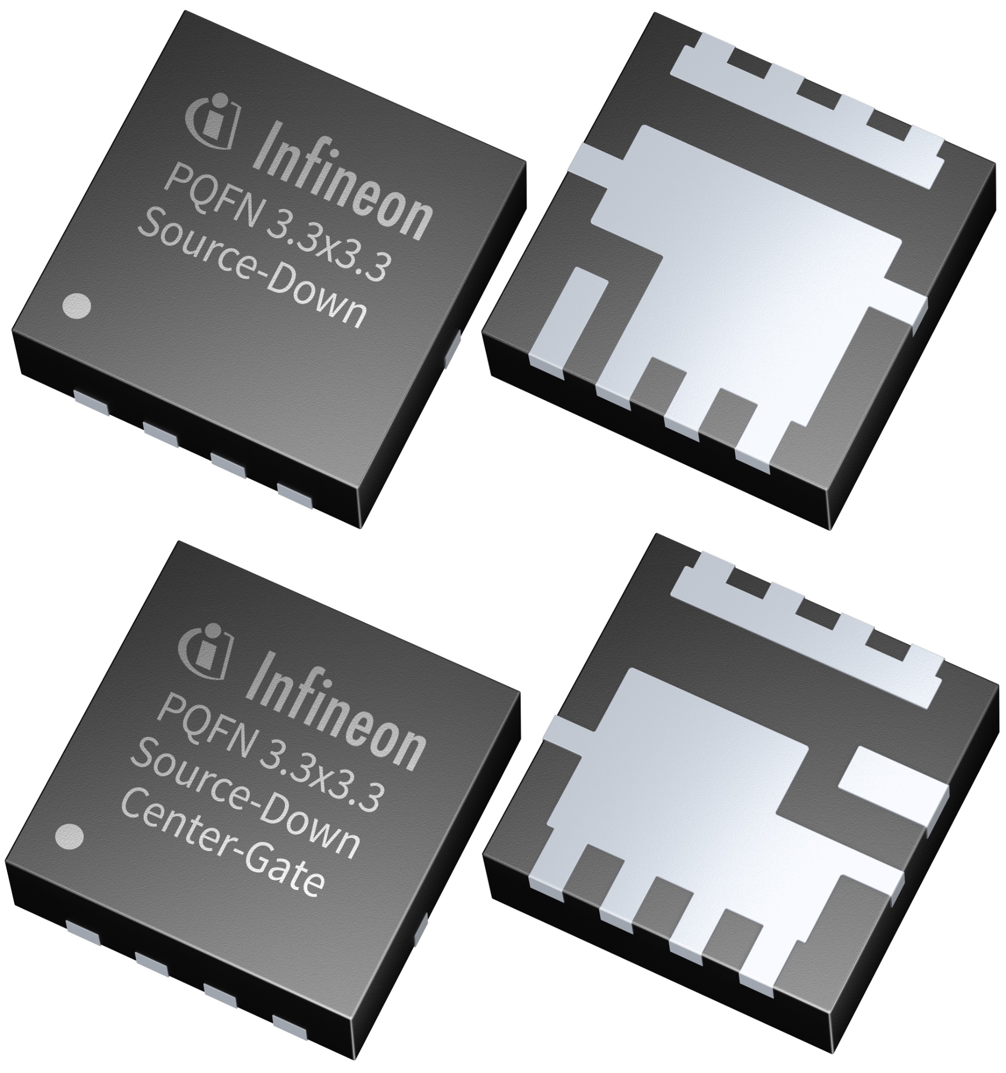
Up to 30 percent reduction in RDS(on) compared to the latest drain-down packages.
Infineon Technologies (Korea CEO Seung-Soo Lee) announced on the 11th that it is launching the next-generation OptiMOS™ Source-Down power MOSFET.
These products are available in a PQFN 3.3mm x 3.3mm package and in various voltage ranges from 25V to 100V.
Setting a new standard in MOSFET performance, this package delivers higher efficiency, power density, superior thermal management and a lower bill of materials.
It is suitable for applications such as motor drives, SMPS for servers and telecom, OR-ing and battery management systems.
Compared to the standard drain-down concept, the latest source-down packaging technology allows for a wider silicon die to fit within the same package outline.
By reducing package losses that limit the overall performance of the device, RDS(on) can be reduced by up to 30 percent compared to the latest drain-down packages.
At the system level, the SuperSO8 5mm x 6mm footprint is PQFN 3.Replacing the 3mm x 3.3mm package allows for a space reduction of approximately 65 percent, enabling a smaller form factor.
By effectively utilizing the remaining space, the power density and system efficiency of the final system can be increased.
Additionally, the source-down concept dissipates heat directly to the PCB through thermal pads instead of bond wires or copper clips.
This simplifies thermal management by improving the thermal resistance RthJC by more than 20 percent from 1.8K/W to 1.4K/W.
Infineon offers two footprint versions and layout options: source-down standard gate and source-down center gate.
The standard gate layout simplifies drop-in replacement for drain-down packages, and the center-gate layout facilitates parallelization.
These two options provide optimal device placement on the PCB, optimization of PCB parasitics, and ease of use.
Comments
Related news
Infineon Supplies Power Solutions to Verizon
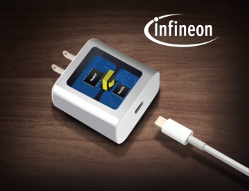
Infineon Technologies (Korea CEO Lee Seung-soo) is supplying power solutions to Verizon, meeting consumer demands for faster charging by delivering higher power through miniaturized chargers.
2021.12.16by 명세환 기자
Infineon's automotive wireless charging security chip meets Qi 1.3 standards.
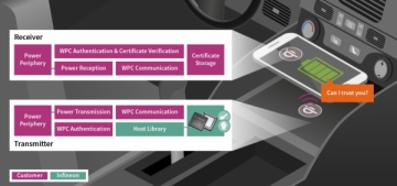
Infineon has introduced a vehicle-grade wireless charging security chip that meets Qi 1.3 certification, reducing customers' security infrastructure investment costs.
2021.12.21by 명세환 기자

Infineon Expands AURIX™ MCU Family
Infineon Technologies (Korea CEO Lee Seung-soo) has expanded its AURIX™ MCU product family, continuing innovation for future mobility.
2022.01.07by 명세환 기자

Intel Unveils Next-Generation 'Core Ultra Series 3' and vPro Platform for Enterprise PCs
Intel has officially unveiled the "Intel Core Ultra Series 3" for next-generation enterprise PCs and the latest vPro platform, addressing a wide range of demands from enterprise notebooks to high-performance workstations.
2026.03.26by 배종인 기자

ROHM Launches ESD Protection Diode Compatible with High-Speed Interfaces of 10Gbps or Higher
Semiconductor specialist ROHM has developed the 'RESDxVx series' of ESD (electrostatic discharge) protection diodes capable of responding to next-generation high-speed data communication environments exceeding 10Gbps, simultaneously enhancing both signal quality maintenance required in high-speed interfaces and IC protection performance.
2026.03.26by 배종인 기자











