



EVG Launches Multifunctional Micro-Nanoimprint Solution 'EVG®7300'
 Published2022.01.19 12:01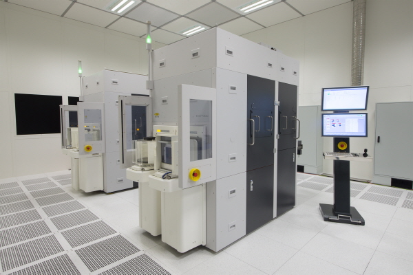
Combination of UV-based processes on a single platform
Available for use in advanced R&D and production processes
EV Group (hereinafter EVG) launches the EVG®7300, an automated SmartNIL® nanoimprint and wafer-level optical system.
EVG is a supplier of wafer bonding and lithography equipment for MEMS, nanotechnology, and semiconductor manufacturing.
EVG's latest solution, the EVG7300, is characterized by combining multiple UV-based processes, such as nanoimprint lithography (NIL), lens molding, and lens stacking (UV bonding), onto a single platform.
This industrial multifunctional system can be used in both advanced R&D and production processes for a wide range of new applications, including micro and nano patterning as well as functional layer stacking.
Examples of such applications include wafer-level optics (WLO), optical sensors and projectors, automotive lighting, waveguides for augmented reality (AR) headsets, biomedical equipment, meta-lenses and meta-surfaces, and optoelectronic devices.
The EVG7300 supports wafers up to 300mm and features high-precision alignment, enhanced process control, and excellent throughput performance.
It also meets the needs of users who wish to mass-produce nano and micro optical components and devices with various degrees of freedom and high precision.
The EVG7300 can be used as a standalone tool or integrated as a module into EVG’s HERCULES® UV-NIL track solution.
EVG’s HERCULES® UV-NIL track solution can add pretreatment or posttreatment processes, such as cleaning, resist coating, and baking, depending on the user’s specific process requirements.
The EVG7300 also provides alignment accuracy (up to 300nm).
This is thanks to a combination of various methods, including an improved alignment stage, a high-precision optical system, multipoint gap control, non-contact gap measurement, and multipoint force control.
In addition, the EVG7300 is a highly flexible platform that supports three process modes (lens molding, lens stacking, and SmartNIL nanoimprint) and wafer sizes ranging from 150mm to 300mm.
The EVG7300 provides a highly efficient platform that meets the manufacturing requirements of the industry's emerging WLO products with rapid stamping and wafer loading, high-speed alignment optics, high-power curing, and a miniaturized tool footprint.
EVG is currently accepting orders for the system and is demonstrating the product at the NILPhotonics® Competency Center located at its headquarters.
Thomas Glinsner, Director of Technology at EV Group, stated, “The EVG7300, our latest nanoimprint solution, combines lens molding and lens stacking with EVG’s proprietary SmartNIL full-field imprint technology on a single platform,” adding, “It provides the flexibility to enable customers to use it in both R&D and mass production processes.”
Comments
Related news

EVG Develops New Display Coating Technology in Collaboration with National Nanotechnology Center and Others
EV Group (EVG) has announced the direction of a joint development program (JDP) for producing improved transparent nanostructured anti-reflective coating for displays, in collaboration with the Nano Comprehensive Technology Center (NNFC), which is a nanotechnology R&D hub for academia, research institutes, and industry, and Nano Initiative (NI), a total solutions company spun off from NNFC that provides raw material manufacturing and process services, including current preliminary results. The three-party collaborators proceeding with the joint development program have successfully demonstrated nanostructured anti-reflective coating with excellent structural replication that provides transmittance exceeding 97 percent, which is superior to most polymeric coatings, and surface hardness of 3H. In contrast, current thin-film coatings technology provides only 92 percent transmittance.
2016.07.13by 김수지 기자

Intel Unveils Next-Generation 'Core Ultra Series 3' and vPro Platform for Enterprise PCs
Intel has officially unveiled the "Intel Core Ultra Series 3" for next-generation enterprise PCs and the latest vPro platform, addressing a wide range of demands from enterprise notebooks to high-performance workstations.
2026.03.26by 배종인 기자

ROHM Launches ESD Protection Diode Compatible with High-Speed Interfaces of 10Gbps or Higher
Semiconductor specialist ROHM has developed the 'RESDxVx series' of ESD (electrostatic discharge) protection diodes capable of responding to next-generation high-speed data communication environments exceeding 10Gbps, simultaneously enhancing both signal quality maintenance required in high-speed interfaces and IC protection performance.
2026.03.26by 배종인 기자

ST Launches 75V Drive IC Targeting 48V Industrial Motor Driving
ST Microelectronics has unveiled the 'STSPIN9P' series of 75V motor drive ICs tailored for 48V-class industrial drive system design. The new product family is characterized by half-bridge and full-bridge configurations that enable design scalability according to motor type and output conditions. Power supply circuits, protection functions, and current sensing circuits are integrated on-chip to simplify system configuration, and the devices are designed to support applications up to 500W maximum. The company plans to provide reference designs and demo boards to support development and evaluation in industrial automation, robotics, pumps, fans, lighting, and textile machinery.
2026.03.26by 배종인 기자

Nordic supports security updates for the entire lifecycle of IoT devices at a single fixed cost
Nordic Semiconductor, a global leader in low-power wireless connectivity solutions, has unveiled a single fixed-cost licensing model that delivers FOTA (Firmware Over-the-Air) and device management capabilities throughout the device lifecycle via nRF Cloud, and introduced a new firmware update solution to prepare for the enforcement of the European Union's Cyber Resilience Act (CRA).
2026.03.26by 배종인 기자











