



KIMM Successfully Mass-Produces Adhesive-Free Nano-Optical Devices
 Published2022.03.17 16:02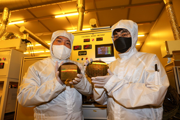
Researchers from the Institute of Machinery and Materials are holding up a nanophotonic device.
The Korea Institute of Machinery and Materials (KIMM), under the Ministry of Science and ICT (President Park Sang-jin), has developed the world's first mass manufacturing technology for chemical adsorption nano-transfer-based nano-photonic devices that do not require adhesive. This is expected to dramatically improve the production process of expensive nano-photonic devices used in various fields, ranging from nano-photodetectors to nano-LEDs and nano-solar cells, thereby increasing economic efficiency.
The Korea Institute of Machinery and Materials (KIMM) announced on the 17th that Director General of the Strategic Coordination Division, Jung Jun-ho, developed an adhesive-free chemical adsorption nanotransfer technology and published the research results in the 16th issue of 'ACS NANO,' a prominent journal in the field of nanotechnology. This research was conducted in collaboration with the research team of Professor Moon-Ho Kim from the Department of Electrical and Electronic Engineering at Nanyang Technological University (NTU) in Singapore.
This study succeeded in developing a chemo-adsorption nanotransfer technology capable of mass-producing high aspect ratio nanostructure-based nanophotonic devices at a low cost. It has been successful to mass-produce high-performance nano-optical devices using only low-cost nano-transfer equipment and wet etching equipment instead of existing high-cost lithography equipment and dry etching equipment.
The chemisorption nanotransfer process developed in this study utilizes the chemisorption phenomenon that occurs when a 20 nm thick layer of gold is deposited on a flexible nanostamp patterned with nanostructures and pressure is applied to a substrate under specific pressure (5 bar) and temperature conditions (160-200℃). When chemisorption occurs, an adhesive force is formed between the gold thin film and the substrate, causing the gold thin film of the nanostamp to be transferred to the substrate.
Until now, expensive dry etching processes were required due to the adhesive between the structure and the substrate, but by utilizing the developed technology, an economical wet etching process called Metal-Assisted Chemical Etching (MAC etch) is possible. The MAC etch process is a wet chemical etching process using a metal catalyst such as gold, in which the substrate is etched through an oxidation-reduction reaction between the substrate immersed in the etching solution and the metal catalyst.
Professor Moon-Ho Kim of Nanyang Technological University (NTU) in Singapore stated, “We fabricated large-area, uniform micro-semiconductor structures on the entire surface of a wafer at low cost,” adding, “We succeeded in securing core technology that enables the uniform production of a large number of devices while minimizing defects.”
"This research achievement is the result of synergy created through international joint research based on the strengths of both institutions, such as KIMM's nano-transfer technology and Nanyang Technological University (NTU)'s wet etching technology," said Jung Joon-ho, Head of the Strategic Coordination Division. "We plan to develop mass manufacturing technologies for nano-LEDs, nano-solar cells, and next-generation batteries through follow-up research."
Meanwhile, this research was supported by the 'Extreme Material Property System Manufacturing Platform Technology' project of the Wave Energy Extreme Control Research Group under the Ministry of Science and ICT.

Comments
Related news
Korea Institute of Machinery and Materials (KIMM) 2021 Best Achievement Award: "Industrial Plasma Source Technology"
The industrial plasma foundational technology has been selected as the top research achievement of 2021 by the Korea Institute of Machinery and Materials (Director Park Sang-jin).
2021.12.22by 배종인 기자
.jpg)
Machinery and Materials Research Institute Reduces Pollutants by 80% by Optimizing Port Loading Equipment
The Korea Institute of Machinery and Materials (KIMM), under the Ministry of Science and ICT, has achieved an 80% reduction in pollutant emissions through port cargo handling equipment optimization technology, with expectations for future domestication of related products and market development.
2022.02.22by 배종인 기자
KIMM, Expanding Display Without Image Distortion
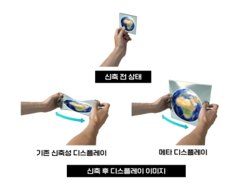
The Korea Institute of Machinery and Materials (KIMM), under the Ministry of Science and ICT (Director Park Sang-jin, hereinafter referred to as KIMM), has successfully developed the world's first stretchable meta micro-LED display technology that expands up to 25% without image distortion, and this is expected to lead to the development of ultra-realistic displays in the future.
2022.03.14by 배종인 기자
Schneider Aims for Building Energy Savings and Operational Stability with Next-Generation HVAC Drives
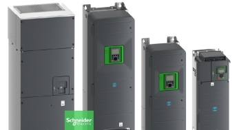
Schneider Electric has unveiled its next-generation HVAC drive product line 'Altivar HVAC'. The new product line's key features center on enhanced energy savings, system operational stability, and building management system integration. The products are divided into 'ATH200' for OEM and small equipment applications, and 'ATH600' for environments requiring continuous operation and advanced control. The company plans to expand the application scope from commercial buildings to facilities where HVAC system stability is critical, such as hospitals, airports, and data centers. The announcement includes over 30% energy savings, operation from -10°C to +60°C, Modbus and BACnet support, and compatibility with low global warming potential refrigerants.
2026.03.26by 명세환 기자
Ecolab Expands AI Data Center Cooling Business Through Acquisition of CoolIT
Ecolab has agreed to acquire CoolIT Systems, a liquid cooling company for AI data centers, for approximately $4.75 billion. The transaction is expected to close by Q3 2026, subject to regulatory approvals. CoolIT has been supplying direct-to-chip cooling-based coolant distribution units, cold plates, and manifolds, serving hyperscale data centers and colocation operators as customers. This acquisition is a measure to address the high-heat and high-density server environments created by AI proliferation. Ecolab plans to combine its water management and digital monitoring capabilities with CoolIT's hardware technology to expand its data center cooling business.
2026.03.26by 명세환 기자











