


UNIST Develops Next-Generation Semiconductor Materials to Overcome Moore's Law Limits
 Published2022.06.03 08:44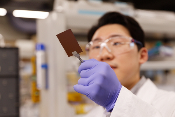
▲First author researcher Ma Gyeong-yeol holds up a substrate coated with hexagonal boron nitride.
Applications Expected in Encapsulation Layers, Membranes, Secondary Batteries, and Quantum Light Sources
UNIST has developed next-generation semiconductor materials capable of overcoming the physical limitations of Moore's Law, and expectations are mounting that this will drive innovation not only in two-dimensional semiconductors but also in encapsulation layers, membranes, next-generation secondary battery electrode materials, and quantum light sources.
UNIST announced on the 2nd that it recently developed synthesis technology for two-dimensional insulator materials to be used in next-generation high-density semiconductors in collaboration with Cambridge University, and published the results in Nature, the most prestigious scientific journal.
This technology is attracting attention as a means to overcome the physical limitations of "Moore's Law," which states that the integration density of semiconductor chip microdevices doubles every two years.
The joint research team from UNIST and Cambridge University used chemical vapor deposition to epitaxially grow a large-area single-crystal triple-layer hBN thin film on a single-crystal nickel (Ni(111)) substrate.
When borazine precursor was exposed to the surface of the single-crystal nickel substrate at high temperature, small hBN crystal fragments were created, and as time passed, the crystal fragments grew and merged into a single-crystal thin film, a process observed with a scanning electron microscope (SEM).
Furthermore, the thickness of the thin film and uniformity over a large area were confirmed using atomic force microscopy (AFM) and Raman spectroscopy analysis methods.
Transmission electron microscopy (TEM) observations confirmed that the grown triple-layer hBN exhibited an epitaxial relationship with the single-crystal nickel, and the atomic arrangement was also regular with a single orientation, confirming it is a single crystal.
Based on the experimental results, theoretical calculations revealed that hBN crystals are formed in only one specific orientation due to step edges present on the single-crystal nickel surface.
The research team also demonstrated that triple-layer hBN single-crystal thin films act as a protective layer for hydrogen-generating catalysts and serve as a barrier to prevent unintended doping in semiconductor devices based on molybdenum disulfide (MoS2), a two-dimensional semiconductor material.
Professor Shin Hyun-seok stated, "Through years of research on boron nitride thin film synthesis, we developed a method to synthesize hexagonal boron nitride, a two-dimensional insulator material, in the form of single-crystal multilayer thin films. As recent research results show that hexagonal boron nitride can be used as an encapsulation layer (protective layer), membrane (proton exchange membrane for hydrogen fuel cells), next-generation secondary battery electrode material, and quantum light source material, active research into high-quality hexagonal boron nitride production technology is necessary for securing original technology."
This research was conducted jointly by Professor Shin Hyun-seok's team from UNIST's Department of Chemistry, Professor Feng Ding's team from the Department of Materials Science and Engineering (Group Leader, IBS Multidimensional Carbon Materials Research Division), Professor Rodney Ruoff's team from the Department of Chemistry (Director, IBS Multidimensional Carbon Materials Research Division), and Professor Manish Chhowalla's team from Cambridge University in the United Kingdom.
The research was supported by the Ministry of Science and ICT-National Research Foundation of Korea's Leaders Research Program, Basic Research Laboratory Program, Future Technology Research Laboratory Program, Sejong Science Fellowship, and the Institute for Basic Science (IBS).

Comments
Related news
UNIST Semiconductor Circuit Design Technology 3, Unveiled at ISSCC
Three semiconductor circuit design technologies from UNIST (President Lee Yong-hoon) will be presented at the 2022 International Solid-State Circuits Conference (ISSCC), known as the "Semiconductor Olympics."
2021.11.23by 배종인 기자
UNIST on the verge of commercializing 6G devices
A UNIST research team has proposed communication device technology capable of rapidly identifying OAM signals by utilizing self-designed metasurfaces, and is drawing expectations that this will accelerate the commercialization of 6G communications.
2022.03.22by 배종인 기자
UNIST develops artificial skin that can hear sound
An interface technology for controlling robots using artificial skin capable of hearing sound has been developed, and it is expected to be applied to avatar robots and other virtual reality, augmented reality, and Internet of Things applications in the future.
2022.03.28by 배종인 기자

Intel Unveils Next-Generation 'Core Ultra Series 3' and vPro Platform for Enterprise PCs
Intel has officially unveiled the "Intel Core Ultra Series 3" for next-generation enterprise PCs and the latest vPro platform, addressing a wide range of demands from enterprise notebooks to high-performance workstations.
2026.03.26by 배종인 기자

ROHM Launches ESD Protection Diode Compatible with High-Speed Interfaces of 10Gbps or Higher
Semiconductor specialist ROHM has developed the 'RESDxVx series' of ESD (electrostatic discharge) protection diodes capable of responding to next-generation high-speed data communication environments exceeding 10Gbps, simultaneously enhancing both signal quality maintenance required in high-speed interfaces and IC protection performance.
2026.03.26by 배종인 기자











