



No charging required, infrared sensor comes out
 Published2022.06.27 14:15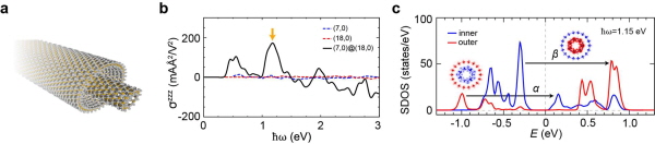
▲ (a) Schematic diagram of the structure of a double-layer TMD nanotube. (b) Shift currents of the single layer and double layer, which were the key focus of this study. It is shown that the shift current of the double layer can generate a photocurrent approximately 20 times greater than that of each single layer (yellow arrow). (c) As a result of analyzing the density of states (SDOS) considering the contribution of the shift current to find the origin of the shift current in the area indicated by the yellow arrow, it was proven that charge transfer between tubes is the key to the very large shift current.
Domestic researchers have identified the bulk photovoltaic effect that occurs when two-dimensional semiconductor materials such as tungsten disulfide are rolled up, raising expectations for the development of new semiconductors, such as new-concept solar cells and infrared sensors that operate without charging.
Professor Park No-jeong's team at UNIST and Professor Kim Jeong-woo of Incheon National University announced on the 27th that they have identified the cause of the increase in bulk photocurrent in multilayer nanotube-shaped tungsten disulfide.
In addition, based on this, a material structure capable of increasing the magnitude of the photocurrent flowing through this semiconductor nanotube by more than 2.5 times was also theoretically proposed.
According to the analysis results, the cause of the increase in photocurrent is charge transport resulting from the multilayer structure of the nanotubes. This multilayer nanotube consists of flat tungsten disulfide rolled up to form a structure similar to tree rings.
In addition, theoretical simulation results were presented showing that if one sulfur (S) atom of tungsten disulfide (WS2) is replaced with selenium (Se), charge transfer between the walls of the multilayer nanotube becomes more active, and this effect can be increased by 2.5 times.
The research team predicts that this discovery will also help in developing new concept solar cell materials to overcome the theoretical efficiency limits of solar cells.
In the field of solar cells, the Shockley-Queisser law—which states that the efficiency of converting sunlight into electricity can never exceed 33.7%—has been absolute. This is due to the limitations of the pn junction used to apply a potential difference. In pn junction solar cells, increasing the current reduces the voltage, and increasing the voltage reduces the current. On the other hand, the bulk photovoltaic effect makes it possible to increase both the current and the voltage simultaneously.
The research team explained, “This achievement is thanks to our ability to perform density functional calculations, which can accurately analyze the electronic structure inside semiconductor materials that change in real time as they absorb light,” adding, “It will be helpful in developing novel solar cells, infrared sensors that operate without charging, and next-generation semiconductor devices.”
This research involved the participation of researcher Bum-Seop Kim from the Department of Physics at UNIST. The research results were published on June 10 in Nature Communications, a prestigious multidisciplinary journal. The research was conducted with support from the National Research Foundation of Korea.

Comments
Related news
UNIST Develops Next-Generation Semiconductor Materials to Overcome Moore's Law Limits
UNIST has developed next-generation semiconductor materials capable of overcoming the physical limitations of Moore's Law, and expectations are mounting that this will drive innovation not only in two-dimensional semiconductors but also in encapsulation layers, membranes, next-generation secondary battery electrode materials, and quantum light sources.
2022.06.03by 배종인 기자
UNIST Develops Low-Power, Ultra-High-Speed 6G Semiconductor Devices
Professor Myung-su Kim from the Department of Electrical and Electronic Engineering at UNIST has jointly developed a low-power, ultra-high-speed analog switch with research teams from the United States, France, and Israel.
2022.06.07by 김예지 기자
Hyundai Motor Group and UNIST Partner to Develop High-Efficiency Solar Cell Devices
UNIST and Hyundai Motor Group held a signing ceremony and unveiling for the 'Hyundai Motor Group-UNIST Joint Research Center for Next-Generation Solar Cells for Mobility (hereinafter Joint Research Center)' on the 10th, announcing the commencement of joint research.
2022.06.13by 성유창 기자

Intel Unveils Next-Generation 'Core Ultra Series 3' and vPro Platform for Enterprise PCs
Intel has officially unveiled the "Intel Core Ultra Series 3" for next-generation enterprise PCs and the latest vPro platform, addressing a wide range of demands from enterprise notebooks to high-performance workstations.
2026.03.26by 배종인 기자

ROHM Launches ESD Protection Diode Compatible with High-Speed Interfaces of 10Gbps or Higher
Semiconductor specialist ROHM has developed the 'RESDxVx series' of ESD (electrostatic discharge) protection diodes capable of responding to next-generation high-speed data communication environments exceeding 10Gbps, simultaneously enhancing both signal quality maintenance required in high-speed interfaces and IC protection performance.
2026.03.26by 배종인 기자











