


Samsung Electronics to Invest 20 Trillion Won by 2028 to Establish High-Tech Research Complex
 Published2022.08.22 11:18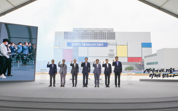
▲ (Center) Samsung Electronics Vice Chairman Lee Jae-yong and the executive team are posing for a commemorative photo at the groundbreaking ceremony for the Samsung Electronics Giheung R&D Complex.
Vice Chairman Lee Jae-yong Attends Groundbreaking Ceremony and Inspects Next-Generation Semiconductor Development
Samsung Electronics plans to invest approximately 20 trillion won by 2028 to secure next-generation advanced semiconductor technology.
Samsung Electronics held a groundbreaking ceremony for its next-generation R&D complex at the Samsung Electronics Giheung Campus in Yongin, Gyeonggi Province on the 19th.
About 100 executives and employees attended the event, including Samsung Electronics Vice Chairman Lee Jae-yong, DS Division Head Kyung Kye-hyun, DS Division CTO Jung Eun-seung, Samsung Advanced Institute of Technology President Jin Kyo-young, Memory Business Division Head Lee Jung-bae, Foundry Business Division Head Choi Si-young, and System LSI Business Division Head Park Yong-in.
The Giheung Campus is where Samsung’s semiconductor business originated in 1983 and where the foundation for a ‘super gap in semiconductors’ was laid, including the development of the world’s first 64M DRAM in 1992, achieving the No. 1 position in the DRAM market in 1992, and achieving the No. 1 position in the memory semiconductor field in 1993.
Samsung Electronics plans to develop the new semiconductor R&D complex in Giheung into a state-of-the-art integrated research and development facility designed to secure a leading position in future semiconductor technology.
The Giheung Semiconductor R&D Complex is built on a scale of approximately 109,000 square meters (about 33,000 pyeong).Samsung Electronics plans to invest approximately 20 trillion won in the construction of a research complex by 2028, including a dedicated semiconductor R&D line scheduled to begin operations in mid-2025.
The R&D complex is expected to serve as a key research base for semiconductor R&D fields, including memory, fabless system semiconductors, and foundry.
The construction of Samsung Electronics' Giheung R&D complex is expected to serve as an opportunity for the domestic semiconductor industry ecosystem to grow to the next level.
Samsung Electronics plans to further strengthen R&D cooperation with domestic and international partners in the materials, equipment, and components sectors through the construction of the Giheung R&D complex.
R&D cooperation with partner companies is expected to lead to the expansion of high-quality jobs and the nurturing of excellent semiconductor R&D talent, thereby contributing to the development of the domestic semiconductor industry ecosystem.
Some equipment and materials partner companies sent video messages congratulating the groundbreaking ceremony and expressing their intention to continue future semiconductor technology cooperation.
Kyung Kye-hyun, Head of the DS Division, reported on the strategy to secure semiconductor technology competitiveness, stating, “We plan to create a virtuous cycle leading to organizational growth through various educational opportunities where excellent R&D personnel can voluntarily gather and grow.”
Following the groundbreaking ceremony, Vice Chairman Lee Jae-yong visited the Hwaseong Campus to hold a meeting with employees and a meeting with the presidents of the DS Division.
Vice Chairman Lee listened to suggestions from employees and exchanged various opinions, including measures to improve organizational culture to promote challenge and innovation.
At the DS Division presidents' meeting held at the Semiconductor Research Institute, key issues and risks surrounding the global semiconductor industry, the progress of next-generation semiconductor technology research and development, and measures to secure technological capabilities to achieve a super-gap were discussed.

Comments
Related news
.jpg)
Samsung Electronics, 2Q sales of 77.2036 trillion won… Highest ever in 2nd quarter
Samsung Electronics achieved record-high operating results for the second quarter in 2022, driven by strong response to server demand in the semiconductor division and expanded supply of system semiconductors.
2022.07.28by 배종인 기자
Samsung Electronics Unveils Next-Generation Memory Solutions
The exponential increase in data is a foreseeable future driven by the expansion of artificial intelligence, metaverse, and 5G/6G technologies. To address this, it is necessary to move away from traditional memory configurations and embrace next-generation memory innovation to meet the big data era. Samsung Electronics, equipped with advanced memory technology capabilities, has unveiled its portfolio and demonstrated its technological prowess.
2022.08.03by 명세환 기자
The 200-Layer NAND Era: Samsung, SK, and Micron's Stacking Competition Heats Up
[Editor's Note] The NAND flash stacking in the semiconductor industry has exceeded 200 layers. Contrary to previous predictions that it would be difficult to exceed 200 layers except for Samsung Electronics, which stacked 128 layers with a single stack, it was Micron from the United States that took the lead in the stacking competition by stacking 232 layers. SK Hynix, not to be outdone, announced the commercialization of 238-layer NAND flash and entered the battle for the top spot in the 200-layer category. Samsung, while appearing to take a wait-and-see approach by mounting its 172-layer seventh-generation V-NAND on UFS 4.0 in early this year, showed confidence by stating that it has already completed securing 200-layer technology. We examined the clash of semiconductor manufacturers in the 200-layer NAND era.
2022.08.12by 명세환 기자

Intel Unveils Next-Generation 'Core Ultra Series 3' and vPro Platform for Enterprise PCs
Intel has officially unveiled the "Intel Core Ultra Series 3" for next-generation enterprise PCs and the latest vPro platform, addressing a wide range of demands from enterprise notebooks to high-performance workstations.
2026.03.26by 배종인 기자

ROHM Launches ESD Protection Diode Compatible with High-Speed Interfaces of 10Gbps or Higher
Semiconductor specialist ROHM has developed the 'RESDxVx series' of ESD (electrostatic discharge) protection diodes capable of responding to next-generation high-speed data communication environments exceeding 10Gbps, simultaneously enhancing both signal quality maintenance required in high-speed interfaces and IC protection performance.
2026.03.26by 배종인 기자











