



Small Business Owners Share Promising New Technologies: Nanoporous Membrane and 3-Terminal Neuromorphic Technology Unveiled
 Published2022.08.24 16:04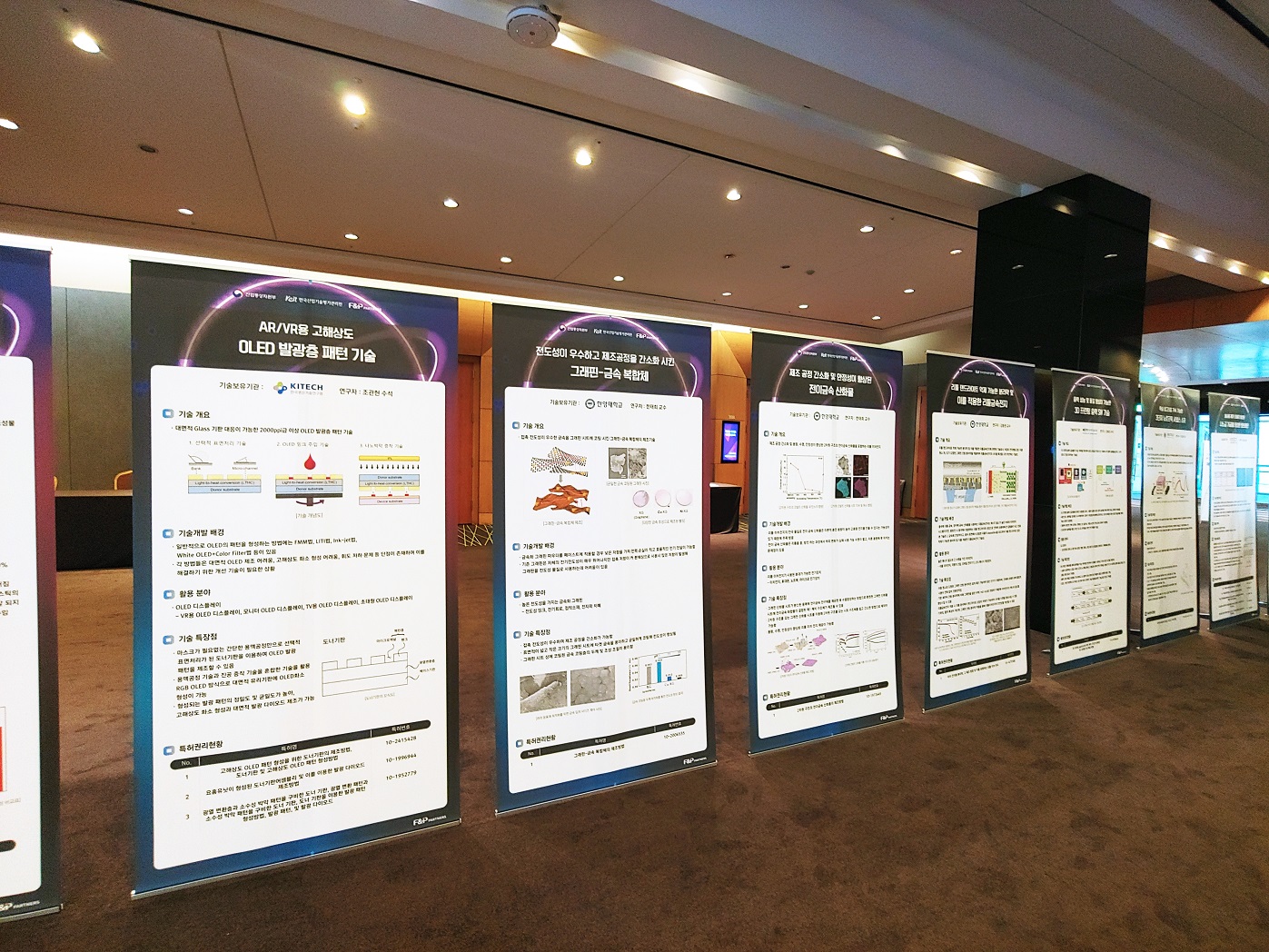
▲제3회 산업기술 R&D 유망기술 발표회
’3단자 뉴로모픽’, CMOS 공정 친화적 소재·학습 알고리즘 가속

산업기술 발전 과정에서 연구개발은 기술 혁신의 근간되며, 산학연의 기술 연구만이 해결 난제들을 극복하는 유일한 길이다. 최근 반도체·디스플레이 관련 소부장 분야에서 산업기술 유망 신기술이 발표돼 R&D 성과를 공유하는 자리가 마련됐다.
한국산업기술평가관리원(산기평)이 23일 코엑스 컨퍼런스룸에서 제3회 산업기술 R&D 유망기술 발표회를 개최했다. 소재·부품·장비 분야 유망 신기술들을 모은 이번 자리는 △반도체 △디스플레이 △이차전지 △3D 프린터 등 다양한 분야에서 발표를 진행했다.
반도체 분야에서는 한국화학연구원 그린탄소연구센터 김인철 책임연구원이 ‘불순물 제거 효율이 향상된 나노기공 멤브레인 필터’를 선보였으며, 경북대학교 산학협력단 전자공학부 우지용 교수가 ‘3단자 뉴로모픽 시냅스 소자 및 제조방법’에 대해 발표를 이어갔다.
■ 나노기공 멤브레인 필터, 불순물 제거로 CMP공정 불량률 최소화
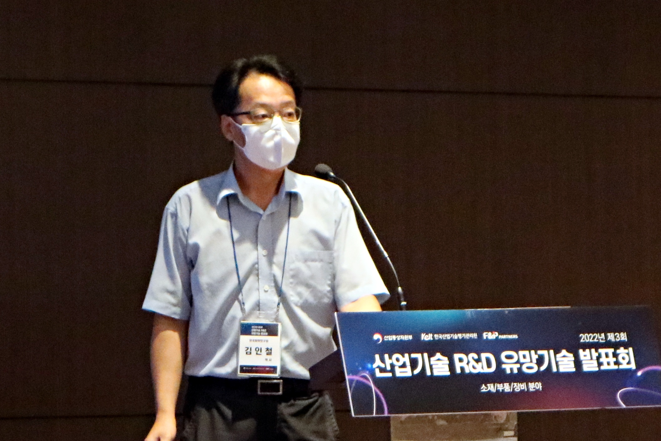
▲한국화학연구원 그린탄소연구센터 김인철 책임연구원
반도체 공정의 미세화가 점차 심화되며 선폭의 감소로 인해 포토레지스트 용액의 불순물 제거가 수율 향상에 중요한 과제로 떠오르고 있다. 불순물은 주로 금속 입자와 유기물 응집 입자로 이뤄져 있으며 이러한 입자들이 미세 스크래치를 내며 패턴 불량을 초래하게 된다.
한국화학연구원 김인철 박사는 “현재 상용화된 나일론 계열 및 폴리올레핀 계열의 멤브레인으로는 포토레지스트 용액의 불순물 제거가 충분히 되기 어렵다”고 설명했다.
이러한 불순물 제거 연구는 삼성전자와 산업부에서 지원한 연구과제로 과거 삼성전자에서 포토레지스트 용액을 수입해 사용하다가 잔존한 불순물들로 인해 생산제품 전량을 폐기한 사건을 계기로 해당 연구를 수행하게 됐다고 밝혔다.
용액 속 하드 파티클은 2나노급 PE필터를 통해 제거가 가능하지만 소프트 파티클은 제거하는 데 한계가 있다고 지적했다. 김 박사는 “미국에서 2나노급 관련 필터를 개발하는 기업에서도 소프트 파티클 제거율이 7%에 불과하다”고 언급했다. 김 박사가 개발한 멤브레인 필터는 나일론66를 사용했을 때 나노입자 제거율이 97%까지 가능했다고 밝혔다.
김 박사는 시제품 제작 및 성능평가까지 마친 TRL 5단계 기술완성도에 이르렀다며, 소프트 파티클 제거가 가능한 멤브레인 필터 기술의 특장점을 설명했다.
팔라듐 나노입자를 이용해 포토레지스트 용액 정제용 멤브레인의 겔 입자 제거 성능을 간단하게 평가 가능하며, 수처리용 멤브레인은 나노급 기공 구조를 가져 내화학성과 투과유량이 우수해 반도체 공정 수처리 장치를 포함한 다양한 수처리 장치에서 사용 가능했다.
또한 큰 기공을 갖는 소수성 지지층과 복수개의 고분자를 이용해 나노급 기공을 형성한 멤브레인을 제조함으로써 불순물 제거 효율을 크게 향상시켰다. 소수성 지지층의 표면 및 단면에 존재하는 공극을 채우면서 소수성 지지층 표면을 친수화시킬 수 있었다.
이러한 기술은 향후 △반도체 공정용 PR정제 △CMP 슬러리 정제 △내화학성 필터 △수처리용 멤브레인 및 필터에 적용 가능한 것으로 전해졌다.
■ 3단자 뉴로모픽, CMOS 공정 친화적 新소재 도입해 인식률 향상
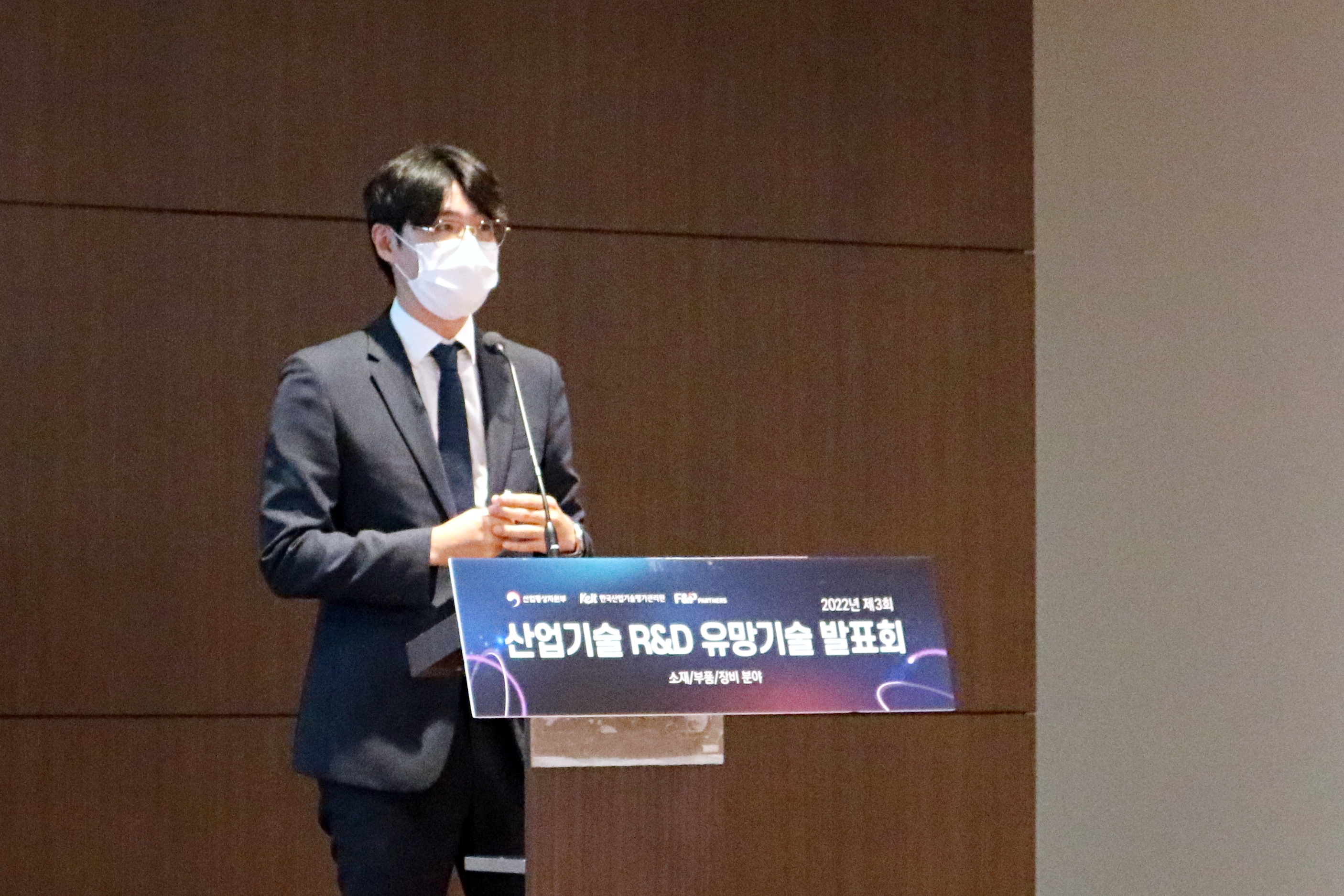
▲경북대학교 산학협력단 우지용 교수
기존 2단자 차세대 메모리 기반 뉴로모픽 반도체는 아날로그 저항상태의 변화가 비선형적이기에 인식률 향상의 한계가 존재해왔다. 이에 모바일 이온 움직임을 이용한 3단자 뉴로모픽 반도체를 개발해 선형적인 아날로그 저항 변화를 확보할 수 있게 됐다.
경북대학교 산학협력단 우지용 교수는 “저항 변화를 유발하기 위해선 모바일 이온 종류와 소재가 반도체 공정에 적합해야 하는데 리튬의 경우는 적합하지 않다”며 “3단자 뉴로모픽 연구에서 반도체 공정에 적합한 소재 발굴에 포커스를 맞춰 연구했다”고 밝혔다.
구리 모바일 이온을 이용하는 등 CMOS 반도체 공정 호환 소재를 찾고 이를 소자 구조에 적용했으며 구리 이온의 주입과 움직임을 제어하는 원천 소재·공정·소자 기술을 TRL 3단계인 연구실 규모에서 성능 검증을 마쳤다.
기존 0과 1의 정보만을 보유하는 휘발성 메모리인 S램, D램 대비 초저전력 아날로그 정보 특성 확보가 가능하다. 우 교수는 “AI구현에 있어서 S램은 3~6개로 만들어 덩치가 크며, D램은 휘발성이기에 전력이 없으면 데이터를 잃어 비휘발성 메모리를 통해 차세대 AI 반도체를 구현하려는 움직임이 크다”고 언급했다.
우 교수가 개발한 차세대 비휘발성 메모리는 1개 소자로 인공지능을 구현해 면적 및 전력 효율이 뛰어나 개선된 성능을 제공할 것으로 전망했다. 차세대 비휘발성 메모리는 높은 선형 특성을 보유해 뉴럴 네트워크 학습 알고리즘 가속에 장점을 가질 것으로 보인다.
이러한 초저전력 초고속 실시간 사물 인식 가능 시스템 구현을 통해 배터리 소모 최소화 및 안정성 높은 자율주행차 구현이 가능할 것으로 전망했으며 △디스플레이 △헬스케어 장비 △로봇센서 등 다양한 스마트 디바이스에서 응용이 가능할 것으로 내다봤다.
가트너에 따르면 세계 인공지능 반도체 시장규모는 연평균 20% 이상의 성장율을 보이며 2020년 230억달러(약 30조원)에서 2026년에는 700억달러(약 93조원)에 이를 것으로 전망했다. AI반도체 응용분야는 통신이 63%로 절반 이상을 차지하며 그 뒤를 컴퓨터 분야가 26%로 뒤를 이었다.
한편, 이날 발표회에는 △구조 및 분자량 제어가 용이한 폴리에테르 폴리올 제조법 △리튬 덴드라이트 억제 가능한 분리막 및 이를 적용한 리튬금속전지 △그래핀-금속 복합체 제조법 △AR/VR용 고해상도 OLED 발광층 패턴 기술 등 다양한 분야의 소부장 유망기술 발표가 진행됐다.

Comments
Related news
Semiconductor Talent ① - Contracted Departments Second Best, Diverse Majors Required
"Semiconductor contract degree programs should be a last resort. It is necessary to nurture semiconductor talent across diverse disciplines." Experts from various sectors gathered to discuss workforce development needed for the semiconductor industry. A wide range of agendas were discussed—from fabless ecosystem personnel to materials, parts and components (MPC), packaging, and regional balanced development—with unified commitment to realizing talent cultivation policies that form the foundation of the semiconductor ecosystem.
2022.07.19by 명세환 기자
Promoting the protection of semiconductor national core technologies
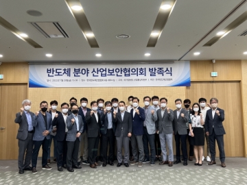
A countermeasure for industrial security in the semiconductor sector has been prepared, including protecting semiconductors as a national core technology, and a consultative body has been established for institutional improvement.
2022.08.02by 배종인 기자
Samsung Electronics to Invest 20 Trillion Won by 2028 to Establish High-Tech Research Complex
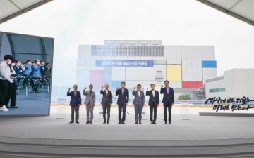
Samsung Electronics will invest approximately 20 trillion won by 2028 to secure next-generation advanced semiconductor technology capabilities.
2022.08.22by 배종인 기자

Intel Unveils Next-Generation 'Core Ultra Series 3' and vPro Platform for Enterprise PCs
Intel has officially unveiled the "Intel Core Ultra Series 3" for next-generation enterprise PCs and the latest vPro platform, addressing a wide range of demands from enterprise notebooks to high-performance workstations.
2026.03.26by 배종인 기자

ROHM Launches ESD Protection Diode Compatible with High-Speed Interfaces of 10Gbps or Higher
Semiconductor specialist ROHM has developed the 'RESDxVx series' of ESD (electrostatic discharge) protection diodes capable of responding to next-generation high-speed data communication environments exceeding 10Gbps, simultaneously enhancing both signal quality maintenance required in high-speed interfaces and IC protection performance.
2026.03.26by 배종인 기자











