



[Korean Institute of Electromagnetic Engineering & Construction Summer Conference] Future of 2.5 and 3D Semiconductors, “Power and Signal Integrity Essential”
 Published2022.08.25 16:00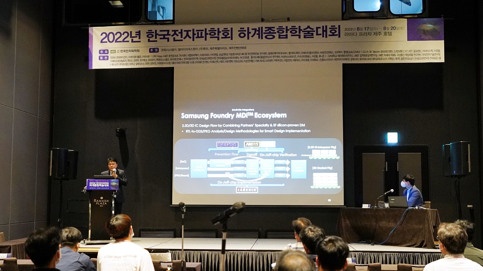
▲ 2022 Korean Institute of Electromagnetic Engineering and Science Summer Conference
Moon Sung-wook, Samsung Electronics Master, "2.5D and 3D Sectors to Grow Significantly"
The global population is approximately 7.7 billion, but the number of devices in use exceeds 500 billion. Unlike the pre-2000s era when per capita PC and mobile phone penetration rates were negligible, semiconductor trends show that starting in 2008, the number of devices surpassed the population, with the average number of devices per person estimated at 15 and projected to reach 1.25 trillion by 2030, according to Cisco Global Cloud Index data.
While semiconductor trends have achieved a twofold performance improvement every two years based on Moore's Law, they have reached technological limits and encountered barriers to innovation such as cost issues and microfabrication limitations. Consequently, various strategies for developing next-generation technologies are currently being explored.
Moon Sung-wook, a Master at Samsung Electronics' Foundry Business Division, delivered a keynote lecture at the Korean Institute of Electromagnetic Engineering and Science Summer Conference titled 'Power & Signal Integrity Technology Challenges for 2.5D and 3D Semiconductor Design Implementation.' On this day, visitors flocked to the event as in-depth presentations were given on Samsung's packaging technology and the challenges of solving power and signal integrity issues.
■ Heterogeneous Packaging Trends: Power and Signal Integrity Essential
One of the reasons behind the emergence of semiconductor heterogeneous integration is the issue of cost. By combining multiple chiplets as building blocks to create a single processor, yield can be increased while costs are lowered, leading many semiconductor manufacturers to adopt this approach.
As advanced node processes have higher unit costs and lower yields, larger dies are more likely to result in defects and consequently greater losses. Therefore, heterogeneous integrated packaging based on a building block approach, which minimizes die size by designing only the necessary chiplets in advanced node processes, is the only way to satisfy both yield and performance.
Morally, integrity means being free from flaws, but in semiconductor design, practical integrity is not a situation of being flaw-free, but rather designing in such a way that even if flaws exist, they do not affect power or signals.
Master Moon Sung-wook defined semiconductor power and signal integrity, emphasizing that this is a field requiring meticulous design down to the minute details.
Integrity must be examined in a diverse and complex manner, including between systems, between transistors, and between modules. In terms of power, issues include voltage drop, switching noise, and crosstalk, while in terms of signal, issues include attenuation characteristics, radio wave reflection, dispersion, interference, and crosstalk.
■ Challenges and Future of 2.5D and 3D Semiconductors
Master Moon Seong-wook mentioned 2.5D silicon interposers and said, “Just a few years ago, the limit for die size was 1,000 mm², but recently, as HBMs have started to fit up to 8 or 12 of them, they are becoming larger to the point where we need to prepare 2,400 mm² or 3,200 mm² in the future.” Consequently, kilowatt-class power is required in data centers.
Master Moon added that due to these power issues, the focus shifts to design implementation using 'decoupling capacitor' solutions, and that resolving heat generation is a major concern for packaging engineers.
Technical challenges in high-performance computing (HPC) include increasing die size and reducing Turn Around Time (TAT) to achieve high performance, high thermal density, yield issues and rapid yield growth due to increased die size, requirements for wide coverage and short TAT due to increased test processes, and multi-die PSI analysis, which remain as future challenges.
3D integrated circuits (ICs) can be utilized in both HPC and mobile applications and offer cost-saving advantages. 3D ICs can also offer advantages in terms of performance and form factor. However, Master Moon noted that there are also many technical challenges, pointing out that the technical challenge surrounding 3D semiconductors is TSV (Through Silicon Via).
Samsung Foundry is demonstrating leadership in building an ecosystem for Multi-Die Integration (MDI) packaging. It develops related tools in collaboration with EDA companies such as Synopsys, Siemens, and Ansys. Specifically, it is collaborating with Synopsys on early-stage noise prevention PSI design solutions, with Ansys on large-scale DB capacity PI/SI solutions, and with Siemens on physical verification and thermal/stress solutions. Moon Master assessed that “tools in the EDA industry are not developing rapidly because the 2.5D and 3D packaging sectors are not mainstream across global industries.”
Master Moon predicted, “We forecast that the 2.5D and 3D sectors will significantly expand in the semiconductor trend,” adding that “extensive preparation will be required amidst existing concerns regarding infrastructure.” He emphasized that Samsung Electronics is proactively preparing for the expansion of the 2.5D and 3D sectors and is already realizing this through some customers.

Comments
Related news
[Electromagnetic Society Summer Conference] 6G, Autonomous Driving, Space, Defense, EMI Radio All-in-One
The electromagnetics field is expanding beyond communications and satellites into diverse applications and convergence areas including electric vehicles, autonomous driving, space and aerospace, defense, medical, and AI, serving as the foundation for next-generation core source technologies. The Korean Institute of Electromagnetic Engineering and Science, which leads related agendas, hosted a summer comprehensive academic conference, providing a venue for academic exchange across industry, academia, and research institutes, which has recently concluded successfully.
2022.08.22by 명세환 기자
[Electromagnetic Society Summer Conference] Active research on wireless charging of electric vehicles, FOD and P2PS
In wireless charging systems for electric vehicles where the power transmitter and receiver are separated, research on FOD and P2PS technologies is being actively conducted to prevent accidents that may occur and to improve charging efficiency.
2022.08.22by 성유창 기자
[Electromagnetic Society Summer Conference] Wayvis, “The only GaN semiconductor fab in Korea”
Gallium nitride (GaN) semiconductors, recognized as a next-generation semiconductor device, serve as a core component in low-power solutions. With high power efficiency and the capability to operate at higher frequencies, voltages, and temperatures with lower power loss, the related market is showing a trend of gradual expansion.
2022.08.23by 명세환 기자
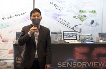
[Electromagnetic Engineering Society Summer Conference] SensorView, “Partner Enhancing RF Engineer Performance”
As the advancement of next-generation 5G and 6G communications is anticipated, market demand for electromagnetic wave solutions is growing. With communication technology-based services and products such as connected vehicles, Internet of Things (IoT), and smart factories and cities rapidly increasing, innovative startups with less than 10 years of history equipped with 5G infrastructure and wireless device solutions are entering the competition with their technological capabilities at the forefront.
2022.08.24by 명세환 기자

Intel Unveils Next-Generation 'Core Ultra Series 3' and vPro Platform for Enterprise PCs
Intel has officially unveiled the "Intel Core Ultra Series 3" for next-generation enterprise PCs and the latest vPro platform, addressing a wide range of demands from enterprise notebooks to high-performance workstations.
2026.03.26by 배종인 기자











