



Possibility of practical application of flexible 'organic semiconductors' opens up
 Published2022.08.30 08:26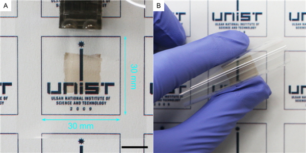
▲Synthesis photograph of HP-FAN in film form
The possibility of applying lightweight and flexible 'organic semiconductors' to actual semiconductor devices has opened up. This is thanks to the synthesis of a new '2D organic semiconductor material' that compensates for performance limitations compared to 'inorganic semiconductors' such as silicon.
Professor Paek Jong-beom's team from the Department of Energy Chemical Engineering at UNIST (President Yong Hoon Lee) announced on the 30th that they synthesized 'HP-FAN (H.P.-PAN) 2D organic polymer structure' through 'aromatic cyclization reaction'.
This material has 'band-gap' suitable for semiconductor applications and high on/off ratio and charge carrier mobility, showing prospects for practical application as an actual semiconductor device.
Currently used 'silicon semiconductors (inorganic semiconductors)' are rigid and heavy, making it difficult to apply them to 'rollable displays' or 'wearable electronics'.
'Graphene', which is lightweight, flexible, durable, and has excellent electrical conductivity, received attention as an alternative semiconductor material, but it also had problems.
The issue is that graphene's band-gap is too small, resulting in a low on/off ratio, and ultimately making it difficult to control current flow within the semiconductor.
Research on 'organic semiconductors' is actively proceeding as an alternative to overcome graphene's limitations. Organic semiconductors are not only as flexible and lightweight as graphene, but also have low processing costs and easy material property control. However, in organic semiconductors, electrons or holes move slowly within the material, making it difficult to apply them as semiconductor devices. When semiconductor devices are made from materials with low charge carrier mobility, electrical signal transmission slows down and problems such as color conversion delays occur in displays.
Professor Paek Jong-beom's team devised a new structure to increase the charge carrier mobility of organic semiconductors. By reacting two types of chemicals (HAB, hexaaminobenzene, DHBQ, dihydroxybenzoquinone), they obtained the HP-FAN structure. This structure has uniform pores and nitrogen (N) atoms added to the 2D aromatic structure, providing appropriate band-gap, high on/off ratio, and charge carrier mobility.
Dr. Noh Hyuk-jun, the first author, explained, "We developed a stable and highly crystalline 2D structure and confirmed the semiconductor characteristics of this material through both experiments and calculations. It showed excellent performance when applied as an actual semiconductor device, presenting the direction for future material development research."
Professor Paek Jong-beom, the research director, said, "We have overcome both the chronic problem of 'low charge carrier mobility' when using 2D polymers as organic semiconductor materials and the fatal limitation of 'low on/off ratio' of graphene semiconductors. We expect significant progress in developing organic semiconductor device materials that will surpass graphene, which is called a 'dream new material'."
This research was conducted jointly with Professor Jo Kil-won's team from the Department of Chemical Engineering at POSTECH. The paper was published on August 30 in Chem, a sister journal of the prestigious international academic journal Cell. The research was supported by the Ministry of Science and ICT's Leaders in INnovation Fostering (LINF) Program (Creative Research), the Center for University-wide Research Facilities (SRC), and UNIST's U-K Brand Development Project.

Comments
Related news
Inorganic-based semiconductors to rise "also cheaper"
Adhesive health monitoring devices and foldable and rollable displays require flexible semiconductors. Most flexible semiconductors are organic-based, but a research team at UNIST's School of Advanced Materials Engineering has developed an inorganic-based flexible semiconductor. Since it can withstand high-temperature, high-pressure processes and exhibits good durability, it is expected to be applicable to the development of various flexible devices.
2021.05.17by 이수민 기자
UNIST Semiconductor Circuit Design Technology 3, Unveiled at ISSCC
Three semiconductor circuit design technologies from UNIST (President Lee Yong-hoon) will be presented at the 2022 International Solid-State Circuits Conference (ISSCC), known as the "Semiconductor Olympics."
2021.11.23by 배종인 기자
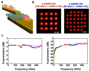
UNIST Develops Low-Power, Ultra-High-Speed 6G Semiconductor Devices
Professor Myung-su Kim from the Department of Electrical and Electronic Engineering at UNIST has jointly developed a low-power, ultra-high-speed analog switch with research teams from the United States, France, and Israel.
2022.06.07by 김예지 기자
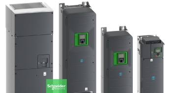
Schneider Aims for Building Energy Savings and Operational Stability with Next-Generation HVAC Drives
Schneider Electric has unveiled its next-generation HVAC drive product line 'Altivar HVAC'. The new product line's key features center on enhanced energy savings, system operational stability, and building management system integration. The products are divided into 'ATH200' for OEM and small equipment applications, and 'ATH600' for environments requiring continuous operation and advanced control. The company plans to expand the application scope from commercial buildings to facilities where HVAC system stability is critical, such as hospitals, airports, and data centers. The announcement includes over 30% energy savings, operation from -10°C to +60°C, Modbus and BACnet support, and compatibility with low global warming potential refrigerants.
2026.03.26by 명세환 기자
Ecolab Expands AI Data Center Cooling Business Through Acquisition of CoolIT
Ecolab has agreed to acquire CoolIT Systems, a liquid cooling company for AI data centers, for approximately $4.75 billion. The transaction is expected to close by Q3 2026, subject to regulatory approvals. CoolIT has been supplying direct-to-chip cooling-based coolant distribution units, cold plates, and manifolds, serving hyperscale data centers and colocation operators as customers. This acquisition is a measure to address the high-heat and high-density server environments created by AI proliferation. Ecolab plans to combine its water management and digital monitoring capabilities with CoolIT's hardware technology to expand its data center cooling business.
2026.03.26by 명세환 기자











