


1nm semiconductors are just around the corner
 Published2022.09.05 15:37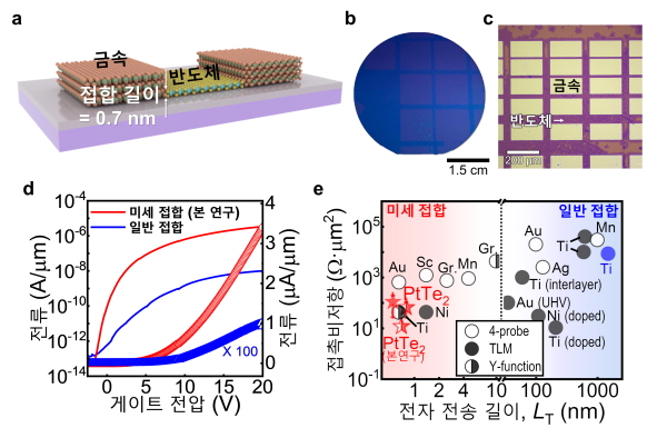
▲2D telluride-based micro-bonding and high-performance semiconductor implementation
Miniaturization and high integration of high-performance semiconductor devices
The development of a 1-nanometer semiconductor is just around the corner, as a research team at UNIST (President Yong-Hoon Lee) has reduced the distance between semiconductors and metals in semiconductor devices to less than 1 nanometer (nm, 1 billionth of a meter).
A research team led by Professors Kwon Soon-yong and Lee Jong-hoon of the Department of Materials Science and Engineering at UNIST (President Lee Yong-hoon) announced on the 5th that they have succeeded in synthesizing (patterning) a “high-performance ultra-thin film semiconductor” device in a desired shape, in which a semiconductor material and an “ultra-fine metal electrode” are horizontally bonded with a gap of 0.7 nanometers (the size of 3 atoms).
To improve the performance of semiconductor chips, the individual components that make up the chips must be made extremely small. A new method has been developed to address this issue. It is expected to accelerate the miniaturization of semiconductor components.
Semiconductor devices function properly only when electrons move to specific locations and directions at the desired times. However, when individual components are made smaller to fit more components into a single chip, a phenomenon occurs where electrons flow to undesirable locations (tunneling effect).
To solve this problem, research is being conducted on 'very thin two-dimensional semiconductor materials', but 'suitable electrodes' have not been developed.
For example, using common metals like titanium (Ti) as electrodes in two-dimensional semiconductor materials can create various defects, degrading performance. Furthermore, common metal electrodes are not only large but also have electron transfer lengths of tens to hundreds of nanometers, increasing the overall size of the semiconductor device.
Ultimately, to realize high-performance ultra-fine semiconductor devices, new two-dimensional electrode materials suitable for them must also be developed, and this study has developed a technology that satisfies this need. For reference, the electron transport length is the length of the path through which electrons can actually move at the junction of a metal and a semiconductor. The shorter this length, the easier it is to avoid performance degradation of semiconductor devices due to miniaturization of the metal electrode.
The team of Professors Kwon Soon-yong and Lee Jong-hoon discovered a way to naturally bond a 'two-dimensional metal electrode' suitable for a high-quality 'two-dimensional semiconductor' during the chemical synthesis process.
The two-dimensional semiconductor material, molybdenum sulfide compound (MoS₂), was chemically synthesized on the edge surface of the two-dimensional metal, platinum telluride compound (PtTe₂).
“General two-dimensional metals are unstable at high temperatures, making it difficult to create various devices. However, two-dimensional platinum telluride (PtTe₂) is stable even at high temperatures of 825 degrees Celsius, making the process possible even at the high temperatures required to synthesize two-dimensional semiconductors,” said Dr. Seung-Wook Song of the Department of Materials Science and Engineering at UNIST, the first author. “This is a technology that implements a defect-free ‘two-dimensional semiconductor-metal junction device’ using chemical vapor deposition.”
Since the semiconductor material was naturally synthesized on the edge of the side of the metal electrode, the bonding surface between the two was thin, about three atoms thick, and almost no defects occurred during the device synthesis process. Thanks to this, the energy barrier (Schottky barrier) at the interface between the metal and semiconductor was very low, close to the theoretical value, and electron movement became easier.
It easily follows the ideal 'Schottky-Mott condition'.
Using this technology, the research team created a two-dimensional metal pattern on a two-inch commercial silicon wafer and chemically assembled a two-dimensional semiconductor using this as a template.
This allows for the synthesis of 'aligned two-dimensional semiconductor-metal junction devices' by arranging the two-dimensional semiconductors along the pattern of the two-dimensional metal.
It is closer to mass production for commercialization because it is a process of manufacturing on a large area on a commercial silicon wafer rather than at the level of a piece of a sample as before.
Professor Kwon Soon-yong said, “Horizontal metal-semiconductor junctions can be arranged in a desired shape and size, allowing for precise and systematic device measurement depending on the semiconductor size.” He added, “In particular, the contact resistance and electron transfer length of the semiconductor-metal junction in the atomic layer transistor are the smallest among the two-dimensional devices implemented so far, which will be helpful in implementing next-generation semiconductors with excellent performance in ultra-fine integrated circuits.”
This achievement was published in the international academic journal 'Nature Communications' on August 22, and was supported by the Nano and Material Technology Development Project and Mid-career Researcher Support Project of the Ministry of Science and ICT and the National Research Foundation of Korea, the IBS Center for Multidimensional Carbon Materials, and the UNIST Future Leading Specialization Project.

Comments
Related news
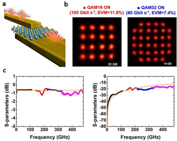
UNIST Develops Low-Power, Ultra-High-Speed 6G Semiconductor Devices
Professor Myung-su Kim from the Department of Electrical and Electronic Engineering at UNIST has jointly developed a low-power, ultra-high-speed analog switch with research teams from the United States, France, and Israel.
2022.06.07by 김예지 기자
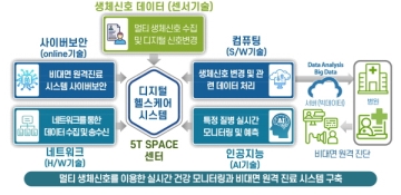
UNIST Launches Full-Scale Research on Telemedicine System
UNIST (President Yong-hoon Lee) is accelerating research into non-face-to-face medical consultation systems, with expectations for fostering digital talent centered on smart healthcare and improving the social value of medical technology.
2022.06.27by 배종인 기자
UNIST and Ulsan University Join Hands to Foster Medical Scientists
UNIST and the University of Ulsan College of Medicine are joining hands to cultivate biomedical scientists who will lead technological innovation from an engineering perspective, and expectations are mounting that this will contribute to future medical industry innovation and enhancement of national competitiveness.
2022.07.11by 배종인 기자

Intel Unveils Next-Generation 'Core Ultra Series 3' and vPro Platform for Enterprise PCs
Intel has officially unveiled the "Intel Core Ultra Series 3" for next-generation enterprise PCs and the latest vPro platform, addressing a wide range of demands from enterprise notebooks to high-performance workstations.
2026.03.26by 배종인 기자

ROHM Launches ESD Protection Diode Compatible with High-Speed Interfaces of 10Gbps or Higher
Semiconductor specialist ROHM has developed the 'RESDxVx series' of ESD (electrostatic discharge) protection diodes capable of responding to next-generation high-speed data communication environments exceeding 10Gbps, simultaneously enhancing both signal quality maintenance required in high-speed interfaces and IC protection performance.
2026.03.26by 배종인 기자











