


ETRI Localizes World-Class GaN Power Devices
 Published2022.09.22 08:38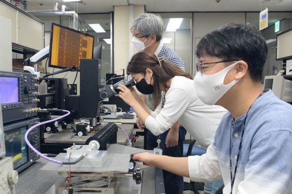
▲ Analyzing the S-band 300W Gallium Nitride (GaN) power device developed by ETRI researchers
Domestic researchers have succeeded in developing gallium nitride (GaN) power devices, considered key components of next-generation semiconductors, using purely domestic technology. This is expected to significantly contribute to enhancing the competitiveness of Korea's semiconductor industry and securing technological leadership.
The Electronics and Telecommunications Research Institute (ETRI) announced that it has developed world-class 'S-band 300-watt (W) class gallium nitride power device technology'.
Gallium nitride is suitable for high-voltage power semiconductors because it has a breakdown voltage more than three times higher than that of silicon (Si), which is commonly used as a semiconductor device, making it advantageous for high-voltage operation, and it does not require a separate energy storage space due to its very fast switching speed.
In addition, it can achieve power density and power efficiency more than seven times higher than gallium arsenide (GaAs), making it suitable for improving communication system efficiency and miniaturization.
For this reason, it can be applied to military radars requiring high power output, high-frequency communication systems, and power systems for electric vehicles.
It is attracting attention as a next-generation semiconductor device with high potential for future industrial and military applications.
In particular, the technology developed this time is a Gallium Nitride Integrated Circuit (MMIC) for AESA radar, a core technology for military fighter aircraft that has been developed and possessed only by the United States and Japan.It is also applicable to [another area], and is expected to contribute significantly to localization and strengthening competitiveness in the defense sector.
Countries such as the United States and Europe have been leading the technological development of gallium nitride power devices.
Due to the nature of the technology, which has high military utility, there were many restrictions on the purchase, utilization, and processing of the components.
ETRI has developed world-class gallium nitride power device technology by designing a gallium nitride high electron mobility transistor (HEMT) structure that simultaneously satisfies high power and high efficiency.
The research team packaged the developed power device chip and verified the performance of the gallium nitride semiconductor device with an output power of 300W and a power density of over 10W/mm.
It is a world-class level that surpasses the performance of existing commercial gallium nitride semiconductor devices of approximately 8.4 W/mm.
Furthermore, this is highly significant in that it was developed entirely using purely domestic technology, from design to process, measurement, and packaging.
The research team expects that by developing world-class gallium nitride power device technology using domestic capabilities, they will be able to reduce dependence on foreign semiconductor materials and narrow the technology gap.
The research team stated that they were able to achieve this result based on human and material know-how accumulated over more than 25 years of research on compound semiconductors, as well as ETRI's equipment and facilities capable of designing and fabricating semiconductor power devices.
Kang Dong-min, Head of the RF/Power Components Research Lab at ETRI, said, “I consider it very meaningful that we have succeeded in securing world-class high-output gallium nitride semiconductor power device technology using domestic technology.” "We hope that this technology will contribute to the localization of key semiconductor components, thereby enhancing the competitiveness of the semiconductor industry and helping to reduce dependence on foreign semiconductor materials," they stated.
The outlook for the gallium nitride power device market is also bright.
According to market research firm Yole Development, the market is projected to grow at an annual rate of 59% from $120 million last year to reach $2 billion by 2027.
The research team plans to enhance the output of gallium nitride semiconductor devices in the future, while also pursuing follow-up research to expand to the 5G 28GHz frequency band.
In addition, research on the localization of key semiconductor components, such as defense radar and communications and 6G next-generation mobile communications, as well as the development of gallium nitride-based integrated circuits, which are one of Japan's major export-restricted items, will be intensified.
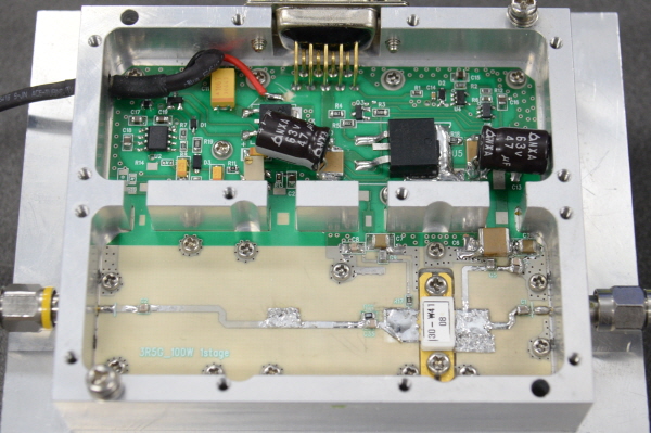
▲ Performance verification module for the developed S-band 300W Gallium Nitride (GaN) power device

Comments
Related news
.jpg)
ST, Full-scale Attack on GaN Power Semiconductor Market
STMicroelectronics (hereinafter referred to as ST), a global semiconductor company supporting diverse electronic applications and customers, extensively supports consumer, industrial, and automotive applications through its GaN (Gallium Nitride) based products.
2022.01.04by 명세환 기자

SiC·GaN, Rapidly Emerging Key Automotive Power Semiconductors
With the widespread electrification of vehicles, compound power semiconductors such as SiC and GaN are rapidly emerging as key components in automobiles to enhance battery efficiency and minimize power consumption.
2022.02.15by 성유창 기자

Infineon Invests 2 Billion Euros in SiC and GaN… Strengthens Leadership in Power Semiconductors
Infineon Technologies (CEO Lee Seung-soo, Korea) is strengthening its power semiconductor market leadership through enhanced wide bandgap (SiC and GaN) semiconductor production capacity.
2022.02.21by 강정규 기자
ST Achieves RF GaN-on-Si Prototype Technology and Performance Milestones
Competition in technology required for building 6G communication infrastructure beyond 5G is making progress. While early-generation RF power amplifiers have been led by LDMOS, RF GaN-on-Si technology, which offers superior RF characteristics and output performance, is demonstrating results at the prototype stage, with R&D accelerating toward mass production.
2022.06.07by 명세환 기자
[Electromagnetic Society Summer Conference] Wayvis, “The only GaN semiconductor fab in Korea”
Gallium nitride (GaN) semiconductors, recognized as a next-generation semiconductor device, serve as a core component in low-power solutions. With high power efficiency and the capability to operate at higher frequencies, voltages, and temperatures with lower power loss, the related market is showing a trend of gradual expansion.
2022.08.23by 명세환 기자











