



Samsung Electronics to mass produce 1.4nm chips by 2027
 Published2022.10.04 10:52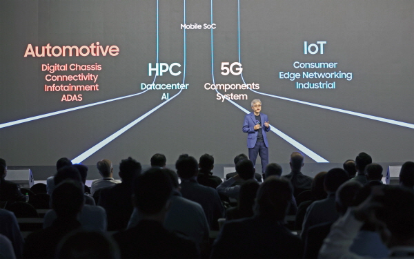
Promoting diversification of applications by process, expanding non-mobile applications by more than 50%.
Samsung Electronics is moving to secure technological leadership through technological innovation in the foundry process, including announcing mass production of 1.4 nanometers by 2027.
Samsung Electronics held the 'Samsung Foundry Forum 2022' in Silicon Valley, USA on the 3rd and unveiled new foundry technologies and business strategies.
This year's Samsung Foundry Forum, held offline for the first time in three years, was attended by approximately 500 fabless customers, partners, and collaborators.
Samsung Electronics announced that it will strengthen its foundry business competitiveness by prioritizing foundry technology innovation, providing optimal processes for each application, providing customized customer services, and securing stable production capabilities.
“Our customers’ success is the reason for the existence of the Samsung Electronics Foundry Division,” said Choi Si-young, President and Head of Samsung Electronics’ Foundry Division. “As a partner creating a better future, Samsung Electronics will become a new standard for the foundry industry.”
Samsung Electronics is accelerating the development of next-generation packaging stacking technology along with innovation in its advanced foundry process.
In 2015, it was the first in the world to mass-produce FinFET transistors, and in June of last year, it was the first in the world to mass-produce GAA (Gate All-in-One) transistors. Around) We have started the world's first mass production of the 3nm 1st generation process using transistor technology, and are expanding the application of 3nm based on our advanced mass production know-how.
In addition, we plan to continue to innovate GAA-based process technology and introduce a 2nm process in 2025 and a 1.4nm process in 2027.
Samsung Electronics is accelerating the development of 2.5D/3D heterogeneous integration packaging technology while simultaneously pursuing process innovation.
In particular, Samsung Electronics plans to apply its proprietary MBCFET (Multi Bridge Channel FET) structure to 3nm GAA technology, while also providing 3D IC solutions and high-performance semiconductor foundry services.
Samsung Electronics has continued to innovate in packaging stacking technology, starting with the successful launch of high-bandwidth memory HBM2 in 2015, followed by I-Cube (2.5D) in 2018 and X-Cube (3D) in 2020.
Samsung Electronics plans to mass-produce the u-Bump (micro Bump) type X-Cube in 2024 and introduce the bump-less type X-Cube in 2026.
Samsung Electronics plans to actively target high-performance, low-power semiconductor markets such as HPC (High Performance Computing), automotive (vehicle semiconductors), 5G, and IoT, and increase the sales proportion of product groups excluding mobile to over 50% by 2027.
Following the world's first mass production of HPC products based on the 3nm process last June, the company is expanding its 4nm process to HPC and automotive applications. We also develop various processes for eNVM (embedded Non-Volatile Memory) and RF to provide foundry services tailored to customer needs.
The company plans to expand its 28nm automotive eNVM solution, currently in mass production, to 14nm by 2024, and is also developing technology for an 8nm eNVM solution in the future.
Samsung Electronics is also expanding its RF process services. Following the 14nm RF process currently in mass production, Samsung Electronics has successfully achieved the world's first mass production of 8nm RF products and is also developing a 5nm RF process.
As of 2022, Samsung Electronics offers over 4,000 IPs to 56 design asset (IP) partners. It also collaborates with nine Design Solution Partners (DSPs) and 22 Electronic Design Automation (EDA) partners. It also offers cloud services with nine partners and packaging services with ten Outsourced Semiconductor Assembly and Test (OSAT) partners.
Samsung Electronics plans to strengthen its customized services with improved performance and functionality, faster delivery, and competitive pricing to discover new fabless customers, while also actively attracting new customers such as hyperscalers and startups.

Comments
Related news
Samsung to invest 450 trillion won in semiconductors and new growth IT over 5 years
Samsung's global standing has been elevated further following U.S. President Biden's visit to Samsung Foundry, and attention is focused on the company's vision for future growth. Samsung has announced that it aims to expand job creation to one million people through achieving status as a semiconductor superpower and fostering new growth engines for the future, bringing expectations for domestic economic stimulus.
2022.05.24by 명세환 기자
Samsung's Super Gap, World's First GAA-Based 3nm Semiconductor Mass Production Begins
Ten years ago, Samsung held only about 1% of the global foundry market share, but has now narrowed the gap enough to challenge TSMC, the current foundry leader. Within five years of launching Samsung Electronics' foundry business division, the company unveiled the world's first GAA-based 3-nanometer process and is demonstrating a pace in process miniaturization that is at least one step ahead of TSMC.
2022.06.30by 명세환 기자
Samsung Electronics Ships First 3nm Semiconductor
Samsung Electronics, which became the first to begin mass production of 3-nanometer semiconductors, held a product shipment ceremony, demonstrating its technological capabilities in the global foundry market.
2022.07.25by 명세환 기자

Intel Unveils Next-Generation 'Core Ultra Series 3' and vPro Platform for Enterprise PCs
Intel has officially unveiled the "Intel Core Ultra Series 3" for next-generation enterprise PCs and the latest vPro platform, addressing a wide range of demands from enterprise notebooks to high-performance workstations.
2026.03.26by 배종인 기자

ROHM Launches ESD Protection Diode Compatible with High-Speed Interfaces of 10Gbps or Higher
Semiconductor specialist ROHM has developed the 'RESDxVx series' of ESD (electrostatic discharge) protection diodes capable of responding to next-generation high-speed data communication environments exceeding 10Gbps, simultaneously enhancing both signal quality maintenance required in high-speed interfaces and IC protection performance.
2026.03.26by 배종인 기자











