



ETRI Develops Ultra-High-Speed Optical Input/Output Semiconductor Using Light
 Published2022.12.22 16:11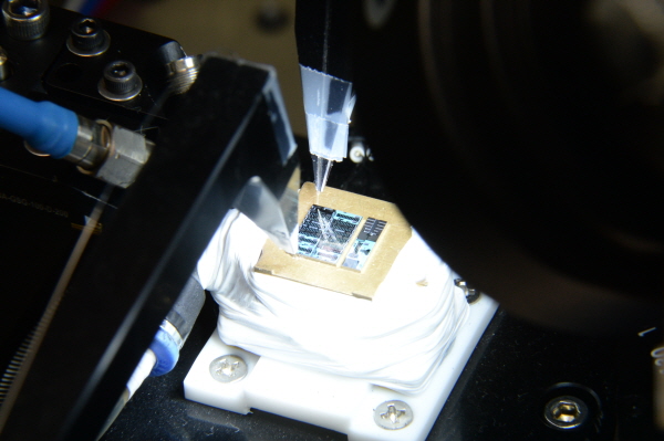
▲ Ultra-high-speed optical input/output semiconductor chip developed by ETRI researchers
Low cost and miniaturization, expected to be utilized in HPC, AI, etc.
Domestic researchers have developed core technology for opto-semiconductors (silicon photonics) that connects semiconductors using light rather than conventional electrical signals. This is expected to be of great help in accommodating the skyrocketing data traffic of the Fourth Industrial Revolution and leading the era of optical communication.
The Electronics and Telecommunications Research Institute (ETRI) announced on the 21st that it has developed a silicon photonics opto-semiconductor chip and related modules capable of transmitting 100 gigabytes (100 Gbps) of data per second in next-generation data centers and high-performance computing networks.
The ultra-high-speed optical communication modules used until now were manufactured by assembling and packaging multiple individual optical components, which resulted in increased costs as the number of channels grew and presented difficulties in expanding transmission capacity and miniaturizing equipment.
In addition, when inputting and outputting data using electrical signals, there were limitations of about 50 Gbps per channel and transmission distances of several tens of centimeters due to bandwidth limitations and excessive power consumption.
On the other hand, by utilizing the opto-semiconductor technology developed by ETRI researchers, transmission capacity and distance can be dramatically increased at a low cost.
Silly developed by the research teamThe cone optical transmitter chip is 2.9x7.3mm and the optical receiver chip is 2.9x3.4mm in size, allowing for miniaturization to 20% of the size of the existing individual optical device assembly method.
Through this miniaturization, multiple optical devices can be integrated into a single chip, solving the problem of expanding communication input/output performance of electronic semiconductor chips that arises as data increases in data centers, high-performance computing, and AI networks.
The performance of semiconductors has also been dramatically improved.
Using the research team's opto-semiconductor chip, data can be transmitted up to 2 km at a speed of 100 Gbps per channel.
It is twice the transmission speed of existing electronic semiconductor chips.
ETRI stated that it was able to achieve this result through a world-class silicon optical modulator capable of transmitting data at a speed of 100Gbps per channel at low voltage, a photodetector with a unique structure capable of high-speed operation by increasing electric field strength, and ultra-high-speed signal processing and signal integrity circuit design technology.
Utilizing the core opto-semiconductor technology developed this time, the research team jointly developed a 100Gbps optical transceiver module capable of transmitting data over 2km in a data center with OISolution Co., Ltd.
In addition, an optical interconnection module capable of delivering 400Gbps performance by linking four channels was also developed and its usability verified.
This achievement has been recognized for the excellence of the research, with five papers published in Optics Express, the most prestigious journal in the field of optical communication, and the company is leading research related to opto-semiconductors, including approximately 35 domestic and international patent applications and 3 technology transfers.
Kim Sun-mi, Head of the Network Research Division at ETRI, stated, “This technology is a core technology for achieving ultra-high-speed, high-capacity optical connections.” "We will proactively develop optical technology required for cloud, artificial intelligence, and ultra-realistic media services, and become a key player in the future era connected by terabit-speed light," he said.
Lee Won-ki, Vice President of OISolution, stated, “Data centers require ultra-high-speed, high-density optical communication technology, and due to high technological barriers, it is a difficult market for domestic companies to enter. Through this technology development, we have secured core silicon photonics technology to enter the global data center market, the largest optical communication market.”
The research team plans to conduct follow-up research to improve the speed per channel of the opto-semiconductor chip to 200Gbps and the transmission capacity to 1.6Tbps, while reducing power consumption to less than half of the existing level and size to about one-ninth.
This technology was developed as part of the Ministry of Science and ICT's 'Development of Core Technologies for Optical Cloud Networking'.

Comments
Related news
ETRI Localizes World-Class GaN Power Devices
Domestic researchers have successfully developed gallium nitride (GaN) power devices, which are considered key components for next-generation semiconductors, using purely domestic technology, and this is expected to significantly contribute to enhancing the competitiveness of Korea's semiconductor industry and securing technological leadership.
2022.09.22by 배종인 기자

ETRI to Release Expanding Displays
Domestic researchers have developed elastic inorganic semiconductor device technology for implementing stretchable displays that can be stretched like rubber bands, and it is expected to lead the next-generation display semiconductor field in the future.
2022.12.08by 배종인 기자
.jpg)
ETRI, Global Cooperation in SiC and 6G Semiconductors
The Electronics and Telecommunications Research Institute (ETRI) has agreed to cooperate with the Korea Advanced Institute of Science and Technology (KAIST) and U.S.-based Coherent on the development of next-generation semiconductor materials and components technology as well as global industrialization efforts.
2022.12.12by 배종인 기자

Intel Unveils Next-Generation 'Core Ultra Series 3' and vPro Platform for Enterprise PCs
Intel has officially unveiled the "Intel Core Ultra Series 3" for next-generation enterprise PCs and the latest vPro platform, addressing a wide range of demands from enterprise notebooks to high-performance workstations.
2026.03.26by 배종인 기자

ROHM Launches ESD Protection Diode Compatible with High-Speed Interfaces of 10Gbps or Higher
Semiconductor specialist ROHM has developed the 'RESDxVx series' of ESD (electrostatic discharge) protection diodes capable of responding to next-generation high-speed data communication environments exceeding 10Gbps, simultaneously enhancing both signal quality maintenance required in high-speed interfaces and IC protection performance.
2026.03.26by 배종인 기자











