



Nepes Secures High-Density, Ultra-Thin 3D Packaging Technology
 Published2023.04.12 16:39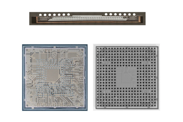
▲Stacked package integrating four layers of DRAM memory and an AI processor (top image - side view, bottom image - front view)
Nepes (CEO Lee Byeong-gu), a leading semiconductor post-processing foundry company, has secured high-density, ultra-thin 3D packaging technology applicable to the production of high-performance artificial intelligence semiconductors, taking a step ahead in the competitiveness of its advanced post-processing platform.
On the 12th, Nepes announced that it had completed the development of 'key materials and process technology for 3D IC manufacturing using FOWLP', a 3D integrated packaging technology, key materials, and test solution applicable to high-performance artificial intelligence semiconductors, together with a joint research group.
The project was led by Nepass and was carried out for approximately five years starting in 2018.
In particular, this research was initiated with the participation of a consortium of numerous organizations, including Microfriend, Chemi, Korea Electronics Technology Institute, Seoul Technopark, Korea Institute of Materials Science, Seoul National University of Science and Technology, and Deoksan Hi-Metal, with the goal of securing the advancement of the Korean semiconductor industry and the competitiveness of advanced post-processing platforms through the development of advanced semiconductor core technologies.
FOWLP (Fan-Out Wafer Level Packaging) is an advanced packaging technology that can integrate multiple chips into a single package. Breaking away from the traditional method of cutting dies and placing them on a substrate to connect them to contact points, it forms electrodes directly on the wafer and packages multiple dies simultaneously.
Since Infineon first successfully implemented it in 2010, it has been used by advanced semiconductor companies such as TSMC.
The main technologies developed in the national project include: △Fan-out based high-density heterogeneous stacking technology, △Large-area EMI shielding and heat dissipation EMC molding package technology, △PSPI polymerization and low-temperature curing insulating film photosensitive material, and △Development of probe cards for fine pitch response.
Based on these technologies, customers can achieve high-density 3D packages with miniaturization and thinning of form factors and excellent heat dissipation and electrical characteristics. It is expected that the use of fan-out technology-based heterojunction technology and large-capacity interface technology will enable the realization of core technologies in areas such as artificial intelligence semiconductors, edge computing, and cloud servers.
Although Korea is a global leader in the memory industry, its influence in the non-memory market, which is more than twice as large, is minimal, with a share of less than 3%.
There are growing voices calling for South Korea to establish a strategy that focuses on securing advanced packaging technology, a key semiconductor process, and fostering a semiconductor industry ecosystem if it is to become a true semiconductor powerhouse.
Accordingly, the research team focused on semiconductor packaging process and material technology to realize the intelligence, low power consumption, weight reduction, and miniaturization of high-performance semiconductors, for which demand is rapidly increasing across application industries such as AI, robotics, and IoT.
Nepes plans to use the package competitiveness it has secured through this project to explore commercialization opportunities with domestic and international artificial intelligence and memory demand companies.
Kim Jong-heon, Vice President of the Technology Development Division, said, “We expect that this national project will contribute to the expansion of new markets in the advanced semiconductor field,” and “Going forward, Nepes plans to lead advanced post-processing technology and further solidify the foundation of the domestic industrial ecosystem.”

Comments
Related news
Nepes to begin production of AI neuromorphic chips in the second quarter
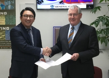
Nexpase and General Vision (GV) have entered into a contract for the development and production of a new artificial intelligence neuromorphic chip and have commenced production. GV, which possesses neuromorphic chip design technology, has designed a new NeuroMem 500 (NM500) chip featuring 576 neurons, and Nexpase holds global exclusive rights for the production, packaging, and sales of this chip.
2017.01.23by 김지혜 기자
AI chip that replicates the structure of the human brain is coming out
"In the era of artificial intelligence, what matters is the chip. There is no longer any place for research based solely on software." At the 'Artificial Intelligence New Industry Convergence Forum' hosted by the Korea Institute of Industrial Technology, Nefes Chairman Lee Byung-gu stated this as a method for democratization, noting that artificial intelligence is drawing closer to our daily lives. Subsequently, Nefes Executive Director Ahn Jeong-ho introduced the artificial intelligence chip 'NM500,' which will be launched next month, saying "there are many advantages when approaching artificial intelligence from a hardware perspective." Nefes is a semiconductor packaging company that designed a system-on-chip (SoC) implementing artificial intelligence by entering into a neuromorphic architecture license agreement with General Vision (GV), a U.S. semiconductor technology company.
2017.06.23by 김지혜 기자

NEPES Showcases Next-Generation Packaging Technology at '2022 ECTC'
Nepes introduces next-generation package solutions at the Korean Society of Electronic Engineers and Technologists, establishing a foundation for new business development and market expansion.
2022.05.31by 배종인 기자

Intel Unveils Next-Generation 'Core Ultra Series 3' and vPro Platform for Enterprise PCs
Intel has officially unveiled the "Intel Core Ultra Series 3" for next-generation enterprise PCs and the latest vPro platform, addressing a wide range of demands from enterprise notebooks to high-performance workstations.
2026.03.26by 배종인 기자

ROHM Launches ESD Protection Diode Compatible with High-Speed Interfaces of 10Gbps or Higher
Semiconductor specialist ROHM has developed the 'RESDxVx series' of ESD (electrostatic discharge) protection diodes capable of responding to next-generation high-speed data communication environments exceeding 10Gbps, simultaneously enhancing both signal quality maintenance required in high-speed interfaces and IC protection performance.
2026.03.26by 배종인 기자











