



'Semiconductor Packaging' Left Behind While Claiming to Become a Semiconductor Superpower
 Published2023.06.08 17:02
Reaching the Limits of Ultra-Miniaturization, Manufacturers Engage in Individual Battles for Packaging Technology Development and Investment
Although the government is calling for the domestic semiconductor industry to become a superpower, there is a growing demand for concrete investment and support plans due to a lack of discussion regarding 'semiconductor packaging,' which will determine the outcome of the future semiconductor market.
The government held the '17th Emergency Economic and Livelihood Meeting: National Semiconductor Strategy Meeting' on the 8th.
This meeting proceeded with key topics including the future sustainability of memory super-gap, strategies for securing competitiveness in system semiconductors, and measures for supply chain risk management and securing technology and personnel.
Regarding the meeting, the Ministry of Trade, Industry and Energy announced that it plans to proceed without disruption with R&D projects totaling 400 billion won for PIM (Processing In Memory) design technology and advanced materials, parts, and equipment technology development, as well as next-generation intelligent semiconductor projects totaling 1.0096 trillion won, in order to maintain a super-gap in memory technology, while also pursuing a preliminary feasibility study worth approximately 1.4 trillion won to preemptively secure promising semiconductor technologies such as power semiconductors, automotive semiconductors, and advanced packaging.
In addition, they announced plans to actively support the timely establishment of newly promoted semiconductor clusters through measures such as timely power supply and expedited licensing.
While it is positive that the government is expressing its determination and commitment to R&D and bold investment to resolve the difficulties facing the domestic semiconductor industry, the industry voices that this is insufficient for the semiconductor packaging sector, which is currently a weak area for the country.br />
It is said to be an empty voice, with only a brief mention that a preliminary feasibility study is planned for advanced packaging, and no one knowing when, where, or how it will be implemented.
At the 'Cutting-edge Chiplet and Packaging Technology Workshop' jointly hosted by the Semiconductor Engineering Society and the Semiconductor Society of the Institute of Electronics and Information Engineers, held at the Korea Semiconductor Industry Association in Pangyo, Seongnam on the same day, Kim Jong-kook, Group Leader of the AVP Business Development Team at Samsung Electronics, attended and announced plans to complete performance testing of basic packaging technology equipped with eight HBMs within the year.
Group Leader Kim Jong-guk stated during the presentation, “In the future, the ability to integrate a large amount of logic and memory into a single package will be the key to semiconductor technology competitiveness.”
As such, semiconductor packaging is attracting attention as a key to Korea's future development into a semiconductor superpower.
This is because the level of semiconductor miniaturization is assessed to have reached its theoretical and technical limits, and as domestic semiconductor makers have focused their investments on miniaturization, there is a growing sense of crisis that they are falling behind global semiconductor companies in the competition for semiconductor packaging technology.
In particular, global advanced semiconductor companies such as Intel, AMD, and TSMC are showcasing advanced technologies for vertical integration of semiconductor chips and packaging different types of semiconductors together, and experts are increasingly calling for advanced semiconductor packaging technology to meet future semiconductor demands, such as AI and autonomous driving.
On the other hand, there has been neglect regarding semiconductor packaging in Korea, such as the absence of a state-led fab for common semiconductor packaging.
Furthermore, domestic semiconductor manufacturers are currently taking the initiative to develop and invest in semiconductor packaging technology on their own.
Accordingly, industry insiders believe that investment in semiconductor packaging must be made now for the future of Korea's semiconductor industry.
Industry officials stated that more concrete discussions regarding investment in semiconductor packaging should take place at future meetings, and emphasized that the government must establish active and specific measures for the sector.
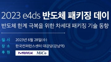
Meanwhile, e4ds will hold the ' 2023 e4ds Semiconductor Packaging Day ' event on June 28 at the Grand Auditorium of the Korea Conference Center. At this seminar, top domestic and international packaging experts from Intel, Nepes, Applied Materials, Hanyang University, and Hyundai Motor Securities are scheduled to present on next-generation packaging solutions. Registration for the event is available on the ' 2023 e4ds Semiconductor Packaging Day ' website ( https://www.e4ds.com/seminar_introduce.asp?idx=137 ).

Comments
Related news
.jpg)
"Advanced packaging is necessary for the semiconductor ecosystem to mature"
As concerns grow that semiconductor fine-process technology is approaching its limits, a forum has been established to discuss the need to develop the semiconductor packaging sector—which is approaching a 100 billion dollar global market—into a next-generation strategic industry.
2022.08.26by 명세환 기자
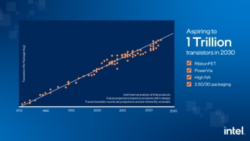
Intel, “Equipped with 1 Trillion Transistors in a Single Package”
Intel has continued to pursue innovations to sustain Moore's Law, setting a target of 10-fold increased density in packaging technology and proposing the use of ultra-thin novel materials measuring three atoms thick for transistor integration.
2022.12.05by 배종인 기자
Overcoming semiconductor limitations is now packaging
Intel, Nexpak, Applied Materials, Hyundai Securities, Next-Generation Intelligent Semiconductor Business Division, and Hanyang University will host the "2023 e4ds Semiconductor Packaging Day," a specialized seminar on semiconductor packaging, on Wednesday, June 28 at the Grand Auditorium of Korea Conference Center.
2023.06.07by 명세환 기자

Intel Unveils Next-Generation 'Core Ultra Series 3' and vPro Platform for Enterprise PCs
Intel has officially unveiled the "Intel Core Ultra Series 3" for next-generation enterprise PCs and the latest vPro platform, addressing a wide range of demands from enterprise notebooks to high-performance workstations.
2026.03.26by 배종인 기자

ROHM Launches ESD Protection Diode Compatible with High-Speed Interfaces of 10Gbps or Higher
Semiconductor specialist ROHM has developed the 'RESDxVx series' of ESD (electrostatic discharge) protection diodes capable of responding to next-generation high-speed data communication environments exceeding 10Gbps, simultaneously enhancing both signal quality maintenance required in high-speed interfaces and IC protection performance.
2026.03.26by 배종인 기자











