


KIMM Develops Next-Generation Semiconductor Large-Area Etching Technology
 Published2023.06.22 09:17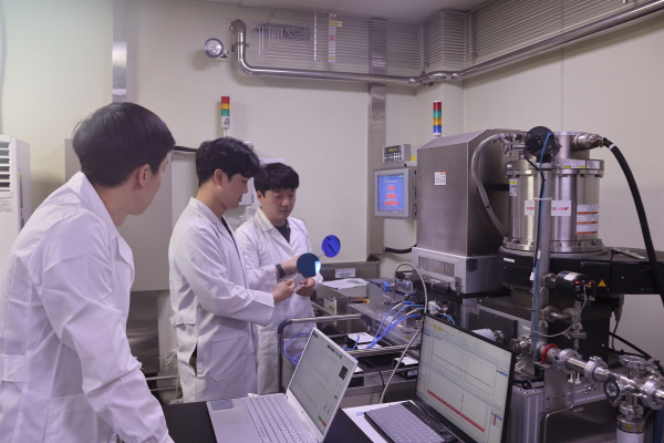
The research team is analyzing the results of the MoS₂ semiconductor process.
The Korea Institute of Machinery and Materials (KIMM), under the Ministry of Science and ICT (President Park Sang-jin), has developed the world's first next-generation 2D semiconductor process technology that offers superior performance and reduced power consumption compared to silicon-based semiconductor technology, amidst global attention on future industries such as artificial intelligence, GPT, the Internet of Things (IoT), and autonomous driving.
A joint research team consisting of Dr. Hyung-Woo Kim from the Plasma Research Laboratory at the Korea Institute of Machinery and Materials (KIMM) and Professor Tae-Sung Kim from Sungkyunkwan University (President Yoo Ji-Beom) announced on the 22nd that they have developed a 4-inch large-area atomic layer etching technology for the next-generation semiconductor molybdenum disulfide (MoS2) using plasma-based reactive ion etcher (RIE) equipment.
In the case of conventional silicon-based semiconductors, as the linewidth of semiconductor chips narrows due to microfabrication, process control down to the atomic level is required. On the other hand, as silicon becomes thinned to atomic layer thickness, precise processing of single-atom thickness is difficult due to the tunneling effect.
Although it was difficult to uniformly form large areas of MoS2-based semiconductors, this study developed a process capable of etching MoS2 to a desired atomic layer thickness over a large area of 4 inches using plasma-enhanced chemical vapor deposition (PVD) equipment and RIE equipment, laying the foundation for mass production of MoS2 semiconductors.
MoS2 can maintain excellent semiconductor performance, with an on/off ratio—a semiconductor performance indicator—that is more than 1,000 times higher than that of conventional silicon. However, there is a disadvantage in that impurities remain on the semiconductor surface during the plasma etching process, requiring an additional process to remove them. The research team solved this problem by introducing a computational science screening system based on Density Functional Theory (DFT).
Kim Hyung-woo, a senior researcher at the Korea Institute of Machinery and Materials, stated, “Recently, the importance of processes capable of controlling the fine linewidth of semiconductor chips has been highlighted in future industries such as AI, GPT, IoT, autonomous driving, and cloud computing.” He added, “Through this technology development, we expect to contribute to the development of the semiconductor industry by improving MoS2 semiconductors to a mass production level using a 2D next-generation semiconductor process.”
This research was selected as a cover article and published in the prestigious international journal 'Chemistry of Materials' in February 2023, and was conducted with support from the KIMM basic project 'Development of Original Technology Based on Plasma Equipment for Core Processes in the Semiconductor and Display Industries'.

Comments
Related news

Intel Unveils Next-Generation 'Core Ultra Series 3' and vPro Platform for Enterprise PCs
Intel has officially unveiled the "Intel Core Ultra Series 3" for next-generation enterprise PCs and the latest vPro platform, addressing a wide range of demands from enterprise notebooks to high-performance workstations.
2026.03.26by 배종인 기자

ROHM Launches ESD Protection Diode Compatible with High-Speed Interfaces of 10Gbps or Higher
Semiconductor specialist ROHM has developed the 'RESDxVx series' of ESD (electrostatic discharge) protection diodes capable of responding to next-generation high-speed data communication environments exceeding 10Gbps, simultaneously enhancing both signal quality maintenance required in high-speed interfaces and IC protection performance.
2026.03.26by 배종인 기자

ST Launches 75V Drive IC Targeting 48V Industrial Motor Driving
ST Microelectronics has unveiled the 'STSPIN9P' series of 75V motor drive ICs tailored for 48V-class industrial drive system design. The new product family is characterized by half-bridge and full-bridge configurations that enable design scalability according to motor type and output conditions. Power supply circuits, protection functions, and current sensing circuits are integrated on-chip to simplify system configuration, and the devices are designed to support applications up to 500W maximum. The company plans to provide reference designs and demo boards to support development and evaluation in industrial automation, robotics, pumps, fans, lighting, and textile machinery.
2026.03.26by 배종인 기자

Nordic supports security updates for the entire lifecycle of IoT devices at a single fixed cost
Nordic Semiconductor, a global leader in low-power wireless connectivity solutions, has unveiled a single fixed-cost licensing model that delivers FOTA (Firmware Over-the-Air) and device management capabilities throughout the device lifecycle via nRF Cloud, and introduced a new firmware update solution to prepare for the enforcement of the European Union's Cyber Resilience Act (CRA).
2026.03.26by 배종인 기자

Practical Training in Low-Noise, Low-Power Circuit Design All in One Place… Training Fee Support
The "2026 Advanced Engineer Practical Masterclass" to strengthen competencies in high-sensitivity analog circuit and sensor-based system design will be held on April 16 at the e4ds Conference Center in Gasan-dong, Seoul. This program will be conducted as an offline paid hands-on training session, not online, and is targeted at engineers seeking on-site intensive learning. Texas Instruments will provide educational support for this training, allowing participation at 150,000 won, a 100,000 won discount from the original price of 250,000 won.
2026.03.26by 배종인 기자











