



KERI Successfully Transfers 'SiC Power Semiconductor Ion Implantation Evaluation Technology'
 Published2023.09.11 15:35
The Korea Electrotechnology Research Institute (KERI) has successfully transferred its 'silicon carbide (SiC) power semiconductor ion implantation evaluation technology' to a Hungarian company, thereby enhancing the price competitiveness of high-performance SiC power semiconductors and contributing to mass production.
KERI announced on the 11th that it recently transferred its "silicon carbide (SiC) power semiconductor ion implantation evaluation technology" to Semilab (Chairman Tibor Pavelka), a semiconductor measurement equipment specialist based in Budapest, Hungary.
Semilab Co., Ltd., with 30 years of experience, has manufacturing plants in Hungary and the United States and is a company holding patents for medium-sized precision measuring equipment and material characterization equipment, possessing the world's best technology in semiconductor characterization equipment technology.
Both parties expect that this technology transfer will enable the standardization of high-quality SiC. Semilab Co., Ltd. plans to develop specialized equipment capable of evaluating the ion implantation process of SiC power semiconductors using KERI technology.
Park Soo-yong, Branch Manager of Semilab Korea, said, “Through the development of specialized equipment, we will be able to lower the defect rate that may occur in the ion implantation process and increase the yield of the device,” adding, “This will serve as a major foundation for stably securing a high-quality ion implantation mass production process with excellent uniformity and reproducibility.”
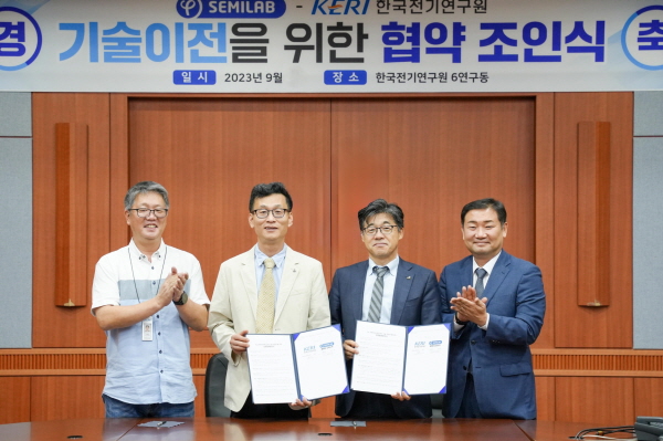
▲ ( From the second from the left) KERI Power Semiconductor Research Group Director Bang Wook, Semilab Korea CEO Park Soo-yong, and other officials are posing for a commemorative photo after signing a technology transfer agreement for 'SiC Power Semiconductor Ion Implantation Evaluation Technology'.
Power semiconductors are core components of electrical and electronic devices, playing a role akin to muscles in the human body by controlling the direction of current and managing power conversion. While there are various materials used for power semiconductors, SiC is receiving the most attention due to its superior material properties, such as high durability and power efficiency. When SiC power semiconductors are installed in electric vehicles, they can reduce battery power consumption and decrease the weight and volume of the vehicle body, potentially leading to an energy efficiency improvement of up to 10%.
While SiC power semiconductors have many advantages, their manufacturing process is also very demanding. Previously, a method was used to form devices by forming an epitaxial layer (a layer forming a single-crystal semiconductor thin film) on a highly conductive wafer (substrate) and passing current through that region. However, during this process, problems arose where the surface of the epitaxial layer became rough and the electron mobility decreased. The high price of the epi wafer itself became a major obstacle to mass production.
To solve this, KERI utilized a method of implanting ions into semi-insulating SiC wafers without an epitaxial layer. Ion implantation, which enables the wafer to be conductive, is the process of breathing life into the semiconductor.
Because SiC materials are hard, it was a difficult technology to implement in practice, as it required ion implantation with very high energy followed by heat treatment at high temperatures to activate them. On the other hand, KERI succeeded in securing related technologies through the operational experience of a SiC-dedicated ion implantation device accumulated over more than 10 years.
Kim Hyung-woo, Head of the Next-Generation Semiconductor Research Center at KERI, stated, “Ion implantation technology can increase the current flow of semiconductor devices and significantly reduce process costs by replacing expensive epi wafers,” adding, “It is a major technology that enhances the price competitiveness of high-performance SiC power semiconductors and contributes to mass production.”
Meanwhile, KERI is a government-funded research institute under the National Science and Technology Research Council of the Ministry of Science and ICT. It boasts the highest level in the country in the field of power semiconductor research, holding over 120 intellectual property rights and achieving technology transfer results of over 3 billion won over the past 10 years.

Comments
Related news

Intel Unveils Next-Generation 'Core Ultra Series 3' and vPro Platform for Enterprise PCs
Intel has officially unveiled the "Intel Core Ultra Series 3" for next-generation enterprise PCs and the latest vPro platform, addressing a wide range of demands from enterprise notebooks to high-performance workstations.
2026.03.26by 배종인 기자

ROHM Launches ESD Protection Diode Compatible with High-Speed Interfaces of 10Gbps or Higher
Semiconductor specialist ROHM has developed the 'RESDxVx series' of ESD (electrostatic discharge) protection diodes capable of responding to next-generation high-speed data communication environments exceeding 10Gbps, simultaneously enhancing both signal quality maintenance required in high-speed interfaces and IC protection performance.
2026.03.26by 배종인 기자

ST Launches 75V Drive IC Targeting 48V Industrial Motor Driving
ST Microelectronics has unveiled the 'STSPIN9P' series of 75V motor drive ICs tailored for 48V-class industrial drive system design. The new product family is characterized by half-bridge and full-bridge configurations that enable design scalability according to motor type and output conditions. Power supply circuits, protection functions, and current sensing circuits are integrated on-chip to simplify system configuration, and the devices are designed to support applications up to 500W maximum. The company plans to provide reference designs and demo boards to support development and evaluation in industrial automation, robotics, pumps, fans, lighting, and textile machinery.
2026.03.26by 배종인 기자

Nordic supports security updates for the entire lifecycle of IoT devices at a single fixed cost
Nordic Semiconductor, a global leader in low-power wireless connectivity solutions, has unveiled a single fixed-cost licensing model that delivers FOTA (Firmware Over-the-Air) and device management capabilities throughout the device lifecycle via nRF Cloud, and introduced a new firmware update solution to prepare for the enforcement of the European Union's Cyber Resilience Act (CRA).
2026.03.26by 배종인 기자
Schneider Aims for Building Energy Savings and Operational Stability with Next-Generation HVAC Drives
Schneider Electric has unveiled its next-generation HVAC drive product line 'Altivar HVAC'. The new product line's key features center on enhanced energy savings, system operational stability, and building management system integration. The products are divided into 'ATH200' for OEM and small equipment applications, and 'ATH600' for environments requiring continuous operation and advanced control. The company plans to expand the application scope from commercial buildings to facilities where HVAC system stability is critical, such as hospitals, airports, and data centers. The announcement includes over 30% energy savings, operation from -10°C to +60°C, Modbus and BACnet support, and compatibility with low global warming potential refrigerants.
2026.03.26by 명세환 기자











