


We listened to feedback from the field to ensure the success of our 100 billion won investment in semiconductor packaging over five years.
 Published2023.12.05 10:29
Promoting R&D to secure cutting-edge packaging source technology
As the government invests 100 billion won over five years to foster advanced semiconductor packaging starting next year, Minister of Science and ICT Lee Jong-ho personally listened to opinions from the field to ensure the success of R&D.
The Ministry of Science and ICT (Minister Lee Jong-ho) inspected the research site for advanced semiconductor packaging substrates at LG Innotek on the 30th and held a meeting with experts from industry, academia, and research institutes.
The Ministry of Science and ICT announced that it plans to launch a new research and development (R&D) project related to advanced semiconductor packaging next year, and that this meeting was held to visit one of the country's leading companies and hear opinions from the field.
This meeting was presided over by Minister Lee Jong-ho, and attended by experts from academia, industry, and research, including LG Innotek CEO Moon Hyuk-soo, Next-Generation Intelligent Semiconductor Business Division Director Kim Hyung-jun, Electronics and Telecommunications Research Institute (ETRI) Vice President Kang Sung-won, and Hanyang University Industry-Academic Cooperation Vice President Lee Ki-hyung. The meeting shared the trends and importance of advanced semiconductor packaging, and based on this, discussed the government's effective research and development (R&D) support policies and fostering plans.
Ahead of the meeting, LG Innotek presented the current status and plans for semiconductor substrate research and development (R&D), emphasizing the necessity and importance of securing core technologies related to advanced semiconductor substrates.
Hwang Pan-sik, Director General of Basic Research Policy at the Ministry of Science and ICT, said, “The government also agrees with the importance and urgency of securing core technologies for advanced semiconductor packaging. To this end, the Ministry of Science and ICT plans to promote R&D, human resource development, and international cooperation projects to secure core technologies related to advanced packaging starting in 2024.”
Dong businessesThis is a project being promoted based on the 'Semiconductor Future Technology Roadmap' prepared by the Ministry of Science and ICT in collaboration with relevant ministries in May of this year. It is expected to invest more than 100 billion won over five years starting in 2024, and the plan is to quickly push forward as soon as the National Assembly's deliberation is completed.
The new advanced packaging project, which the Ministry of Science and ICT plans to support starting next year, aims to secure core technologies related to 3D stacking, high-efficiency and fine-pitch packaging, high-heat dissipation packaging structures, next-generation interposers, and ultra-fine substrate and substrate processes.
In addition, we plan to separately pursue a talent development program to cultivate master's and doctoral level professionals specializing in the field of advanced packaging.
Additionally, an open discussion was held at the symposium on the topic of 'Measures for developing our country's advanced packaging technology to the world's best level.'
Minister Lee Jong-ho emphasized, “Advanced packaging is a key technology to address the limitations of semiconductor miniaturization, and competing countries have already recognized its importance and are actively investing in it at the national level.” He added, “The Ministry of Science and ICT will strive to enhance semiconductor technological competitiveness through active investment in promising next-generation technologies.”
Meanwhile, the Ministry of Science and ICT plans to compile the contents, suggestions, and recommendations discussed at the meeting and actively reflect them in next year's Ministry of Science and ICT advanced packaging project.

Comments
Related news
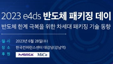
Overcoming semiconductor limitations is now packaging
Intel, Nexpak, Applied Materials, Hyundai Securities, Next-Generation Intelligent Semiconductor Business Division, and Hanyang University will host the "2023 e4ds Semiconductor Packaging Day," a specialized seminar on semiconductor packaging, on Wednesday, June 28 at the Grand Auditorium of Korea Conference Center.
2023.06.07by 명세환 기자
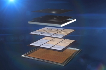
'Semiconductor Packaging' Left Behind While Claiming to Become a Semiconductor Superpower
While the government proclaims the achievement of semiconductor superpower status in the domestic industry, voices are growing louder calling for concrete investment and support plans for semiconductor packaging, which will determine the outcome of the future semiconductor market, as discussions on this matter remain insufficient.
2023.06.08by 배종인 기자
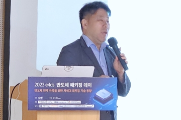
Semiconductor Market Recovery Remains Question Mark This Year… Focus on AI Semiconductors
At the 2023 e4ds Semiconductor Packaging Day, there were forecasts suggesting that the semiconductor market this year may not recover easily.
2023.07.03by 명세환 기자
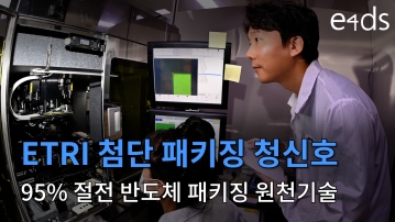
ETRI, Development of 95% Energy-saving Semiconductor Packaging Source Technology
The Electronics and Telecommunications Research Institute (ETRI) has developed an advanced semiconductor chiplet packaging technology that reduces power consumption by 95% by significantly streamlining the existing nine-step process down to three steps.
2023.07.28by 배종인 기자
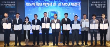
Semiconductor Advanced Packaging, Public-Private Partnership
The Ministry of Trade, Industry and Energy, Samsung Electronics, SK Hynix, LG Chem, Hana Micron, Protec, Sapion Korea, Simtec, the Next-Generation Intelligent Semiconductor Business Division, the Korea Semiconductor Industry Association, the Korea Institute of Industrial Technology Evaluation and Planning, and other companies in the materials, parts and equipment (MPM) sector, semiconductor advanced packaging specialists (OSAT), and fabless enterprises concluded an agreement on cooperation for semiconductor advanced packaging technology development.
2023.08.29by 배종인 기자











