


Nepes aggressively targets AI semiconductors with 8-layer RDL interposer technology.
 Published2024.06.05 09:16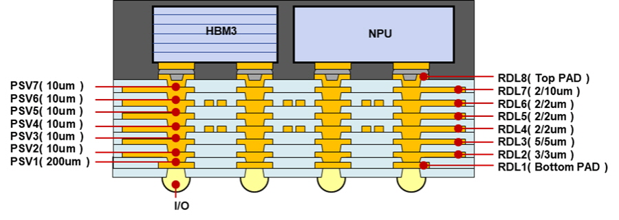
Nepes is aggressively targeting the AI inference market, which has high market growth potential, with its new 8-layer RDL interposer technology.
Nepes announced that it presented its fan-out based RDL interposer technology at the 74th Electronic Components and Technology Conference (ECTC) held in Denver, Colorado, USA from May 28th to 31st (local time).
On the 29th, the second day of the event, Nepes shared the current status of advanced packaging technology with a paper titled ‘Single and Multi NPU Chiplet Heterogeneous Integration Packaging Based on Fan-Out RDL Interposer With Silicon Bridge Technology’ at the Thermo-mechanical Stress and Reliability Analysis for Materials in Future Packaging session.
The technology is characterized by implementing chiplet packaging, which vertically and horizontally connects multiple chips on an interposer, with a fan-out process-based redistribution layer (RDL) interposer instead of a silicon (Si) interposer.
/> With the increasing demand for artificial intelligence semiconductors, chiplet packaging technology has become a major topic of discussion, attracting great interest from field participants due to its advantages such as excellent electrical characteristics, production efficiency, and reduced manufacturing costs.
In particular, at this ECTC, 8-layer RDL interposer technology, which is two layers higher than the existing technology, was developed and shared in a situation where 6-layer RDL interposer technology is common worldwide.
This is significant in that it has changed from a structure that previously required a substrate to a structure that does not require a substrate.
In other words, in the existing case, after the RDL interposer manufacturing, chip bonding, and molding processes, an additional flip-chip process must be performed on the substrate.
On the other hand, the 8-layer process eliminates the need for a flip-chip process on the substrate, enabling packaging without a separate substrate, reducing the overall package size. In addition, the process is simplified, increasing process efficiency, and simplifying the electrical connection with the complex substrate makes it possible to implement excellent electrical characteristics.
A Nepes official said, “RDL interposers are suitable for connecting various chips and are expected to be widely used in areas such as edge computing for inference artificial intelligence, which has great market growth potential in the future.” He added, “We plan to actively pursue commercialization through network strengthening and technology cooperation with customers in the future to secure global semiconductor package competitiveness.”

Comments
Related news
Nepes Secures High-Density, Ultra-Thin 3D Packaging Technology
Advanced semiconductor back-end foundry specialist Nepes (CEO Lee Byung-gu) has secured high-density ultra-thin film 3D packaging technology applicable to manufacturing high-performance AI semiconductors, advancing one step ahead in competitive advantage within advanced back-end process platforms.
2023.04.12by 배종인 기자
Neopass and Seoul Metropolitan Office of Education Join Hands to Revitalize Semiconductor Education
Neopass (Chairman Lee Byung-gu), an advanced semiconductor specialist company, has joined hands with the Seoul Metropolitan Office of Education (Superintendent Cho Hee-yeon) to foster specialized semiconductor technical workforce and establish a vocational education system.
2023.04.25by 배종인 기자
Overcoming semiconductor limitations is now packaging
Intel, Nexpak, Applied Materials, Hyundai Securities, Next-Generation Intelligent Semiconductor Business Division, and Hanyang University will host the "2023 e4ds Semiconductor Packaging Day," a specialized seminar on semiconductor packaging, on Wednesday, June 28 at the Grand Auditorium of Korea Conference Center.
2023.06.07by 명세환 기자
.jpg)
Nepes begins mass production of advanced PMIC packaging
Semiconductor backend processing company Nepes has recently begun receiving orders for power semiconductors for artificial intelligence (AI) chipsets from U.S. global fabless companies, and is now actively expanding into advanced packaging markets including high-performance computing (HPC) and automotive applications.
2024.02.26by 배종인 기자
Nepas, Semiconductor HBM Plating Solution Mass Production Begins in Full Scale
Netpass has been working on the localization of plating solution, a functional semiconductor material that has been entirely dependent on imports, through long-term in-house R&D and collaboration, and has been conducting initial production for the past two years. With its adoption at an HBM TSV factory, the company is now beginning full-scale mass production starting this year.
2024.04.04by 배종인 기자











