


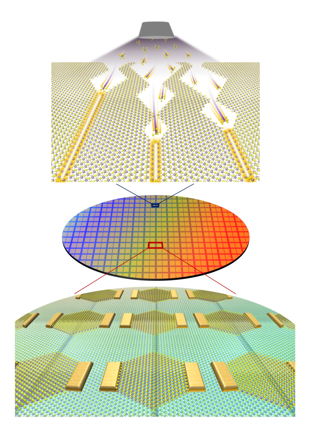
Implementation of ultra-small semiconductor devices with 0.4 nm gate electrodes
 Published2024.07.04 16:21

Comments
Related news

IBS Supercomputer No. 2 'Olaf', Listed as World's 10th Ultra-low-power Supercomputer
The Institute for Basic Science (IBS, Director No Do-young) has registered its second supercomputer, 'Olaf,' as the world's 10th most energy-efficient supercomputer.
2023.11.27by 배종인 기자
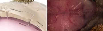
IBS Implements Brain-Computer Interface with Tattoo-Thin Electronic Circuits
The Nanomedicine Research Unit at the Institute for Basic Science (IBS, Director Noh Do-young), led by Principal Investigator Cheon Jin-woo (Distinguished Professor at Yonsei University) and Professor Park Jang-ung (Professor of Materials Science and Engineering at Yonsei University), in collaboration with the research team of Professor Jeong Hyun-ho and Professor Jang Jin-woo from the Department of Neurosurgery at Severance Hospital, has successfully implanted a soft artificial neural electrode resembling brain tissue into the brain of a rat and printed electronic circuits on the skull surface using a 3D printer to achieve long-term transmission and reception of brain waves (neural signals).
2024.03.12by 배종인 기자
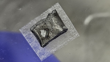
Atmospheric pressure diamond synthesis succeeds, world's first
The Institute for Basic Science (IBS, Director Noh Do-young), led by Principal Investigator Rodney Ruoff of the Multidimensional Carbon Materials Research Unit, has successfully synthesized diamond at atmospheric pressure using a liquid metal alloy composed of gallium, iron, nickel, and silicon—a world first.
2024.04.25by 배종인 기자
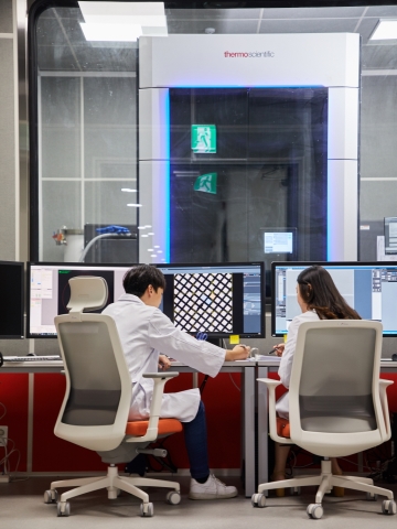
IBS Ultra-low Temperature Electron Microscope Ranks 1st in User Preference for 3 Consecutive Years
The ultra-low temperature electron microscope (Cryo-EM) at the Institute for Basic Science (IBS, Director No Do-young) has been evaluated as the most preferred equipment by researchers in the field, observing living cells like taking a 'snapshot'.
2024.05.17by 배종인 기자
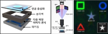
A camera that moves as fast as an eagle's eye has been released
The Institute for Basic Science (IBS, Director Roh Do-young), the Nanoparticle Research Center led by Associate Director Kim Dae-hyung (Professor, Department of Chemical and Biological Engineering, Seoul National University), and Professor Song Young-min's team at Gwangju Institute of Science and Technology (GIST) have jointly developed an object detection specialized camera that mimics the structure and function of a snow eye. The technology is expected to see increased application in unmanned robots, autonomous vehicles, and drones that require object detection capabilities.
2024.05.30by 배종인 기자











