



Keysight Launches 3kV High-Power Wafer Test System
 Published2024.12.12 09:25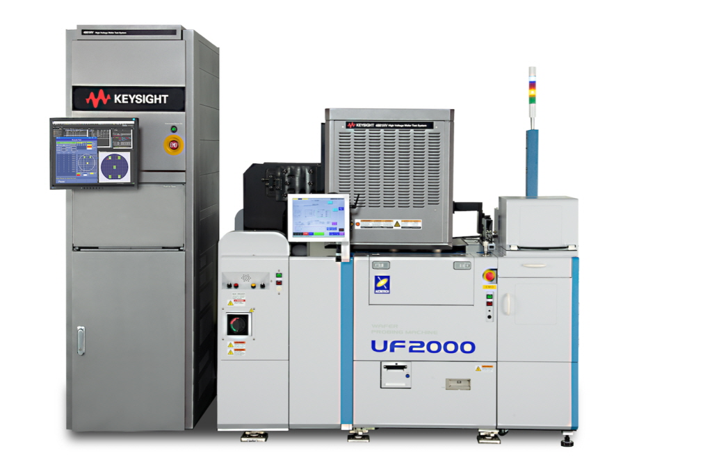
Keysight Technologies launches 3kV high-power wafer test system, expected to improve power semiconductor productivity and efficiency.
Keysight Technologies, Inc. announced today the launch of the 4881HV high-voltage wafer test system, expanding its semiconductor test portfolio.
The system provides parametric test capabilities up to 3kV, allowing high-voltage and low-voltage tests to be performed simultaneously.
This is expected to significantly increase the productivity and efficiency of power semiconductor manufacturers.
Traditionally, manufacturers have used separate equipment for high-voltage and low-voltage testing, but the increasing demand for next-generation devices such as silicon carbide (SiC) and gallium nitride (GaN) has created a need for more efficient test solutions.
Keysight's new test system addresses this challenge and is designed to perform process control monitoring (PCM) and wafer acceptance test (WAT).
The 4881HV high-voltage wafer test system uses a high-voltage switching matrix (HV-SWM) to meet requirements up to 3 kV and is expandable up to 29 pins.
The system supports a wide range of measurements from ultra-low currents to 3kV voltages, and is also capable of high-voltage capacitance measurements and various parametric tests.
Also HV-SWM is suitable for high voltage and low voltage tests.Integrates into one system to reduce installation space and test time, and increase efficiency.
The system is integrated with Keysight's SPECS-FA software to improve the efficiency of the entire production process.
Keysight's new system incorporates protection circuits and control devices to protect operators and equipment from hazards that may occur during high-voltage testing, and complies with safety regulations such as SEMI S2 to ensure stability and reliability.
“Keysight’s introduction of this wafer test system builds on our extensive experience in advanced semiconductor testing,” said Shinji Terasawa, vice president of Keysight’s wafer test solutions business unit. “Our goal is to provide cutting-edge solutions that meet the rapidly changing needs of the semiconductor industry.”

Comments
Related news
.jpg)
Keysight Announces Results of Interoperability Tests Between Etiforce 5G-V2X Modem and Autotalks Chipset
Keysight announced through its official website on the 6th that it has completed the industry's first 5G-V2X (3GPP Release-16 sidelink) interoperability test involving multiple modem vendors.
2024.08.07by 성유창 기자
Keysight Launches Post-Quantum Cryptography Test Solution
Keysight Technologies announced the industry's first post-quantum cryptography (PQC) test automation solution on the 13th. The solution, added to Keysight Inspector, enables device and chip suppliers to identify and remediate hardware vulnerabilities.
2024.08.13by 김예지 기자
Keysight, ETAS, Automotive Cyber Security Agreement
Keysight Technologies (hereinafter Keysight) is collaborating with ETAS to provide comprehensive automotive cybersecurity solutions to automotive manufacturers and automotive suppliers.
2024.08.23by 성유창 기자
Keysight, World's First 3GPP Release 16 Sidelink Wireless Interoperability Connectivity
Keysight Technologies has conducted the world's first 3GPP Release 16 (Rel-16) sidelink radio interoperability test between Effifos SIRIUS 5G-V2X sidelink platform and Autotalks SECTON3 5G-V2X chipset through Keysight PathWave signal generation for NR-V2X and X-Apps for 5G NR V2X modulation analysis measurement applications.
2024.09.04by 배종인 기자
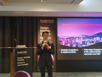
Keysight, “We sincerely invest in technology to connect the world and make it safe in a connected world”
Keysight introduced cutting-edge technologies in telecommunications, automotive, and AI fields on the 16th through "Keysight World Tech Day 2024." On that day, Lee Seon-woo, President and CEO of Keysight Korea, stated, "Keysight is making sincere investments for industrial development so that we can connect the world and ensure that the connected world operates safely."
2024.10.16by 배종인 기자











