


ST to Invest $60 Million to Build Next-Generation PLP Pilot Line in Tours, France
 Published2025.10.30 09:58
Strengthening process, design, and manufacturing innovation capabilities for next-generation chip development in Europe.
STMicroelectronics (ST) is building a new pilot line in Tours, France, strengthening its continued technological innovation and global manufacturing strategy.
STMicroelectronics announced today that it is building a new pilot line for next-generation Panel-Level Packaging (PLP) technology at its Tours, France, facility.
The line is expected to be operational in the third quarter of 2026 and will drive innovation in advanced chip manufacturing technologies through a $60 million investment and collaboration with the local R&D ecosystem.
PLP is a technology that increases manufacturing throughput by utilizing large rectangular panels instead of existing round wafers, and simultaneously realizes miniaturization, high performance, and cost efficiency through automated chip packaging and testing processes.
Building on its first-generation PLP line operating in Malaysia, ST plans to develop next-generation PLP technology at its Tours facility and expand its application across a range of product groups, including automotive, industrial, and consumer applications.
“The development of PLP capabilities at the Tours site will further advance our innovative approach to chip packaging and test manufacturing technology, enhancing efficiency and flexibility,” said Fabio Gualandris, President of ST’s Quality, Manufacturing and Technology Division. “This will enable us to address a broad application portfolio including RF, analog, power and microcontrollers.” “The goal is to expand the application of PLP technology,” he said.
He continued, “We have a team of experts from various fields, including manufacturing automation, process engineering, data science, and product R&D, working together, and this is at the core of ST’s strategic heterogeneous integration initiative.”
Heterogeneous integration is a next-generation chip design method that maximizes performance and efficiency by integrating chips with various functions into a single package, and ST is leading the technology roadmap through this.
ST has already demonstrated its high-performance chip packaging and test capabilities in Europe through its Malta fab, and the pilot line at the Tours facility is part of a strategy to restructure its global manufacturing footprint.
This will strengthen our process, design, and manufacturing innovation capabilities for next-generation chip development in Europe, laying the foundation for long-term success.
This project is expected to maximize synergy effects through collaboration with local research and development institutions, including the CERTEM R&D Center.
Some operations in France and Italy are also being given new roles, as ST's strategy to expand its advanced manufacturing infrastructure gains momentum.
PLP technology is considered a key element that will determine the future of the semiconductor industry, and ST is strengthening its global technology leadership through it.
In particular, by simultaneously securing manufacturing efficiency and flexibility, as well as high-performance chip integration technology, ST is expected to be at the center of the development of next-generation electronic devices.

Comments
Related news
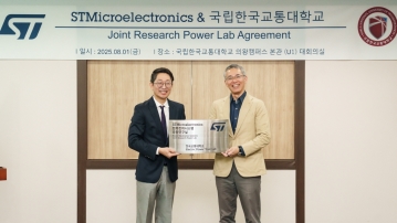
ST and KT&G sign agreement to establish a "Power Lab" to cultivate specialized power semiconductor talent.
Global semiconductor company STMicroelectronics (hereinafter ST) is launching full-scale efforts to cultivate domestic power semiconductor specialists and support product development for domestic customers through the establishment of a 'Power Lab'.
2025.09.16by 배종인 기자
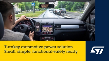
ST Strengthens Competitiveness with Low-Cost Automotive Power Management ICs
Global semiconductor company STMicroelectronics (ST) has launched the SPSA068, a compact and cost-effective power management IC (PMIC) for automotive applications. The SPSA068 is designed to simplify power management for single-supply microcontroller (MCU)-based applications, has obtained AEC-Q100 certification, and supports up to ASIL-B level according to ISO 26262 functional safety (FuSa) standards.
2025.09.24by 배종인 기자
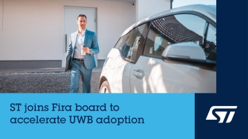
ST accelerates UWB technology expansion and digital key business
Global semiconductor company STMicroelectronics (hereinafter ST) has joined the board of the FiRa® Consortium, which leads the advancement of Ultra-Wideband (UWB) technology, thereby strengthening its influence in the automotive digital key and smart connectivity markets.
2025.09.29by 배종인 기자
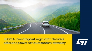
ST Strengthens Vehicle Electrical System Stability
STMicroelectronics (hereinafter ST), a global semiconductor company supporting diverse electronic applications and customers, has launched a new linear voltage regulator (LDO) 'L99VR03' that supports automatic adaptive standby current, wide input voltage, and high-temperature environments, thereby enhancing the stability of automotive electrical systems.
2025.10.01by 배종인 기자
ST Optimizes 48V Automotive Power Architecture
Global semiconductor company STMicroelectronics (hereinafter ST) has launched the 'L98GD8', an 8-channel gate driver optimized for 48V automotive power architecture, contributing to improved efficiency in mild hybrid systems.
2025.10.15by 배종인 기자











